

Adhesive-coated electronic parts on a connection sheet
a technology of electronic parts and adhesives, applied in the direction of paper/cardboard articles, transportation and packaging, other domestic articles, etc., can solve the problems of difficult to use a variety of tape widths, complicated apparatus, and the attraction of adhesives in the use of connection methods, etc., to achieve efficient mounting of electronic parts
- Summary
- Abstract
- Description
- Claims
- Application Information
AI Technical Summary
Benefits of technology
Problems solved by technology
Method used
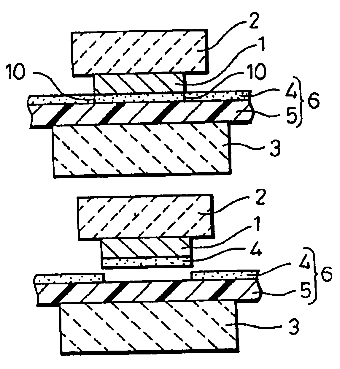
Image

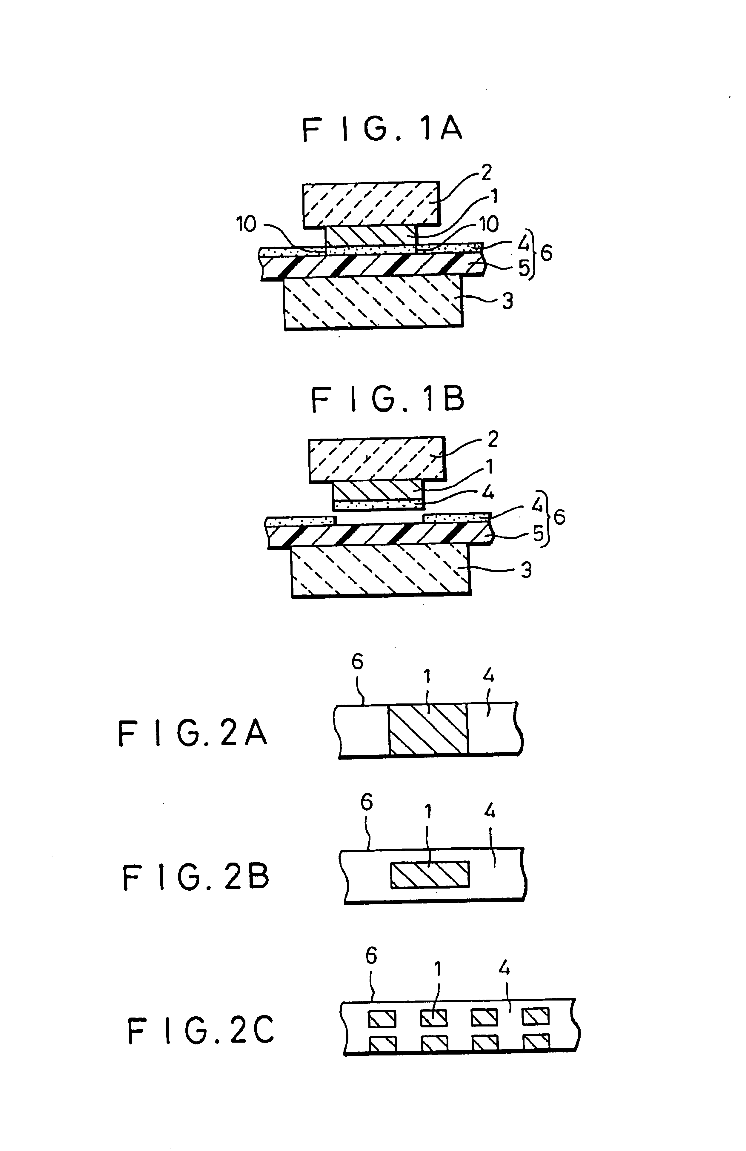
Examples
example 1
(1) Preparation of Adhesive Layer
A solution containing 30% ethyl acetate was obtained by mixing, in the ratio of 30 / 70, a phenoxy resin (polymeric epoxy resin) and a liquid epoxy resin (epoxy equivalent: 185) containing a micro-encapsulated latent hardener. To this solution was added 2 vol % of electrically conducting particles, which were obtained by coating polystyrene particles having a particle size of 3±0.2 μm with Ni and Au in thicknesses of 0.2 μm and 0.02 μm, respectively, followed by mixing and dispersion of the conducting particles. The dispersion was applied to a separator (polyethylene terephthalate film treated with silicone; thickness: 40 μm ) by means of a roll coater, and the separator applied with the dispersion was dried at 100° C. for 20 minutes to obtain an adhesive film with a thickness of 20 μm.
The activation temperature of the adhesive film was measured using a DSC and was found to be 120° C. Using a model composition from which the hardener had been removed, ...
example 2
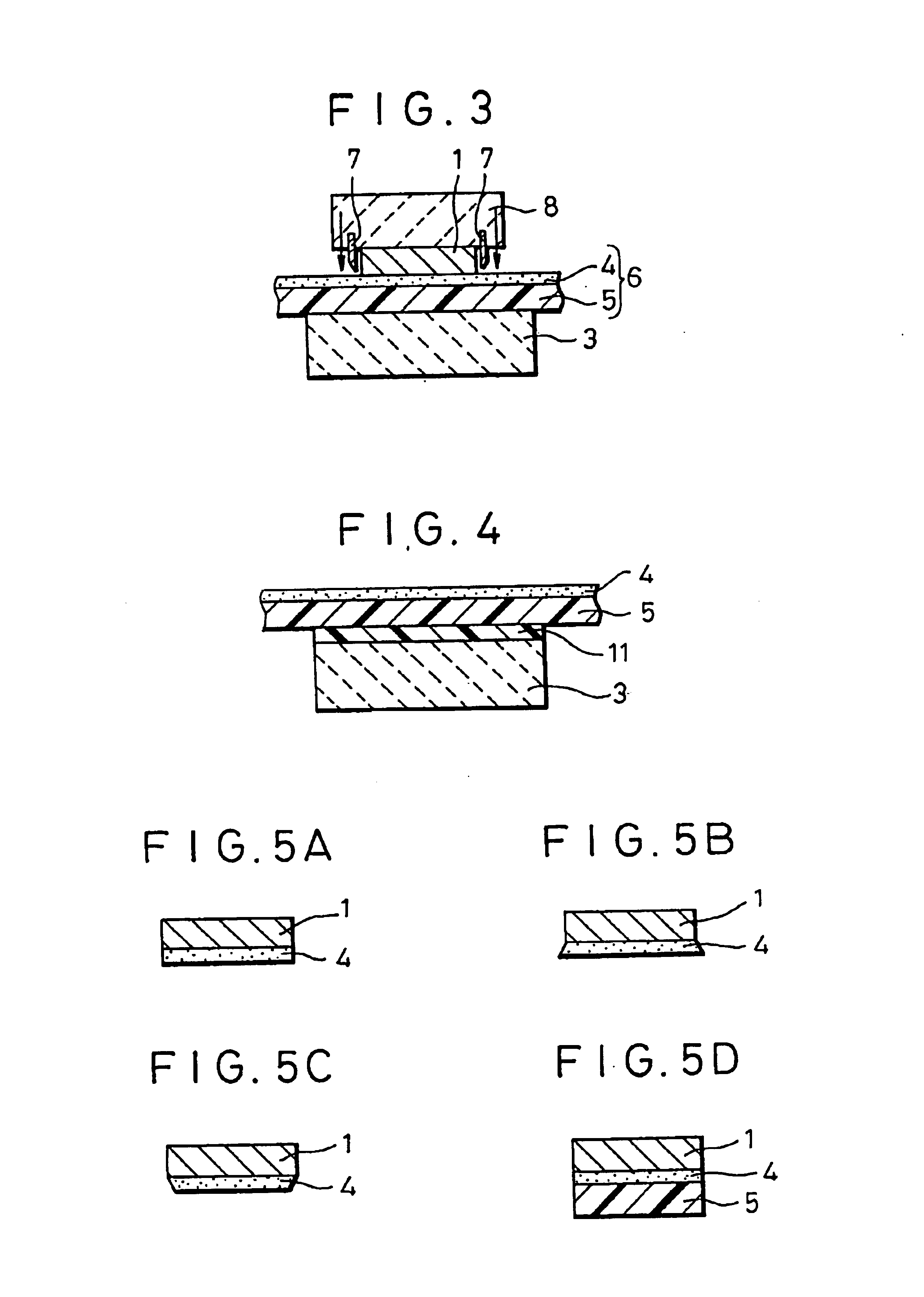
IC chips were mounted on a substrate in substantially the same manner as in Example 1, but the adhesive-coated chips were produced by a different method. Specifically, a pressure head provided with a cutting jig was used, and the tape used had a width of 10 mm. For the 2×10 mm chip, for example, a heater wire comprising a nichrome wire and arranged so as to extend along the four sides of the chip was used as the cutting jig. The pressure head was not heated and was used at room temperature. Since a heater wire was used as the cutting jig, the tape could be cut for the entire depth inclusive of the separator, so that an adhesive-coated chip having a separator affixed to its adhesive layer was obtained. Other chips could also be similarly affixed with adhesive. For the chip of 10 mm in diameter, a looped heater wire with an inner diameter of 11 mm was used as the cutting jig. Also in this case, the electrodes of the individual chips could be satisfactorily connected to the correspondi...
example 3
IC chips were mounted on a substrate in substantially the same manner as in Example 2, but when producing adhesive-coated chips, the temperature of the heating head was set at 70° C. Further, a cutting tool with a straight edge was used as the razor. Also in this case, adhesive-coated chips could be easily obtained. Since both the razor and the heating means were used, the adhesive could be readily transferred to the chips. Furthermore, the heating temperature could be set at a low temperature, as compared with the case of Example 1.
PUM
| Property | Measurement | Unit |
|---|---|---|
| viscosity | aaaaa | aaaaa |
| viscosity | aaaaa | aaaaa |
| thickness | aaaaa | aaaaa |
Abstract
Description
Claims
Application Information