Ferroelectric capacitor and a semiconductor device

a ferroelectric capacitor and semiconductor technology, applied in the field of semiconductor devices, can solve problems such as deterioration of the retention property of ferroelectric films, and achieve the effect of preventing deterioration of imprint properties

Inactive Publication Date: 2005-01-11
FUJITSU SEMICON LTD
View PDF16 Cites 21 Cited by
  • Summary
  • Abstract
  • Description
  • Claims
  • Application Information

AI Technical Summary

Benefits of technology

[0040]It is to be noted that, for the PZT film belonging to the rhombohedral system, a value of remanent polarization is small and therefore a retention property is also lower as compared to the PZT film belonging to the tetragonal system. Accordingly, it can be understood that if such a film having a good imprint property is formed at the upper and lower electrode interfaces, respectively, it is possible to prevent deterioration of the imprint property due to charge accumulation near the electrode interface.

Problems solved by technology

It may be understood that for the ferroelectric film of PZT polycrystals oriented in the direction, when directions of polarization are different between a pair of neighboring domains, strain is accumulated in a domain wall, and a defect due to the strain causes deterioration of the retention property of the ferroelectric film.

Method used


Image

  • Ferroelectric capacitor and a semiconductor device
  • Ferroelectric capacitor and a semiconductor device
  • Ferroelectric capacitor and a semiconductor device

Examples


first embodiment

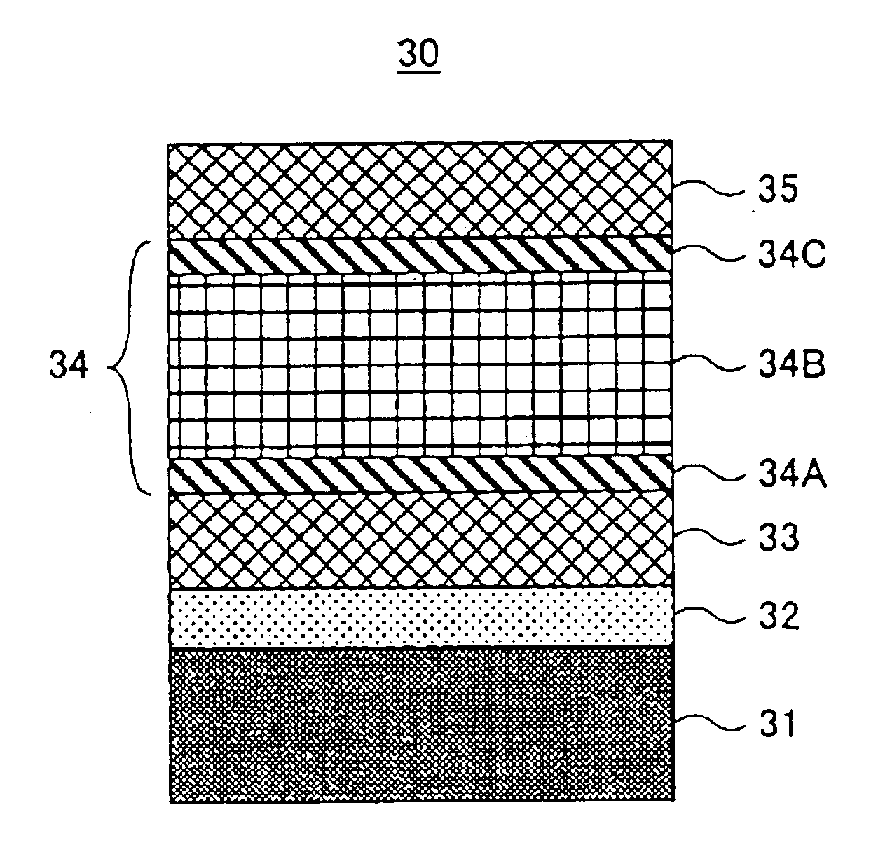
[0059]the present invention will be described with reference to FIG. 10 that shows a ferroelectric capacitor 30 of a first embodiment of the present invention.

[0060]Referring to FIG. 10, a ferroelectric capacitor 30 is formed on a Si substrate 31 via a SiO2 film 32. The ferroelectric capacitor 30 includes a lower electrode 33, a PZT film 34 formed on the lower electrode 33 and an upper electrode 35 formed on the PZT film 34. The lower film 33 is a Pt film that is mainly oriented in the direction and has a thickness of typically about 100 nm.

[0061]The PZT film 34 includes a PZT film part 34A formed at an interface with the lower electrode 33, a PZT film part 34B provided on the PZT film part 34A and a PZT film part 34C provided on the PZT film part 34B at an interface with the upper electrode 35. The PZT film part 34A has a thickness of about 20 nm and is formed of PZT crystals belonging to the rhombohedral system. The PZT film part 34B has a thickness of about 180 nm and is formed ...

second embodiment

[0068]Referring to FIGS. 11A through 11D, a process of fabricating the ferroelectric capacitor 30 of FIG. 10 will be described as the present invention.

[0069]Referring to FIG. 11A, the Si substrate 31 provided with the SiO2 film 32 is subjected to a sputtering process in an Ar atmosphere such that a Pt film serving as the lower electrode 33 is deposited with a thickness of about 200 nm. During the sputtering process, O2 may be introduced in the sputtering atmosphere by an amount that is about 20% of the sputtering atmosphere, such that the produced Pt film is an ordinary film oriented in the normal direction but may be a film oriented in the direction. See, for example, M. H. Kim, et al., J. Mater. Res. Soc. Vol. 14, No. 3 (1999), pp. 634-637.

[0070]In a step shown in FIG. 11B, a sol-gel solution of 2 weight % with a Pb:Zr:Ti ratio of 105:70:30 is applied on the structure shown in FIG. 11A and dried. Then, the structure undergoes a rapid heating process for 60 seconds at 700° C. in...

third embodiment

[0081]Referring again to FIGS. 11A through 11D, a method of fabricating a ferroelectric capacitor of the present invention will be described, wherein the PZT films 34A, 34B and 34C are formed by a CVD process.

[0082]In the present embodiment, the step of FIG. 11A is the same as the previous embodiment. A Pt film oriented in the direction is formed as the lower electrode 33 on the SiO2 film 32 covering the Si substrate 31.

[0083]Then, in the step shown in FIG. 11B, a sample of the structure shown in FIG. 11A is introduced into a processing container of a CVD apparatus (not shown). An internal pressure of the processing container is set to a range between 130 and 1300 Pa and the temperature of the substrate under process is set to a range between 500 to 600° C.

[0084]Under such a condition, Pb(DPM)2, Zr(DMHD)4 and Ti(iPrO)2(DPM)2 diluted with THF are introduced into the processing container as Pb, Zr and Ti vapor phase materials with a flow ratio of 1:0.56:0.46. A carrier gas containing...


PUM


Abstract

A ferroelectric capacitor includes a lower electrode, a ferroelectric film provided over the lower electrode and having a perovskite-type structure and an upper electrode provided over the ferroelectric film. The ferroelectric film includes a first ferroelectric film part having a first crystal system and formed along at least one interface with at least one of the lower electrode and the upper electrode and a second ferroelectric film part having a second crystal system that is different from the first crystal system.

Description

BACKGROUND OF THE INVENTION[0002]1. Field of the Invention[0003]The present invention relates to a semiconductor device and particularly relates to a semiconductor device having a ferroelectric capacitor.[0004]Semiconductor memory devices such as DRAMs and SRAMs are widely used as high-speed main memory devices for information processing devices such as computers. However, such semiconductor memory devices are volatile in nature and thus information stored thereon is lost when the power supply is turned off. Non-volatile magnetic disk devices are commonly used as large-scale auxiliary storage devices for storing programs and data.[0005]However, magnetic disk devices are bulky, vulnerable to mechanical shocks and have a large consumption power. A further drawback of magnetic devices is a slow access speed during information read / write operations. In order to obviate such drawbacks, recently, EEPROMs or flash memories that store information by accumulating electric charges on floating...

Claims


Application Information

Patent Timeline
Patent Type & Authority Patents(United States)
IPC IPC(8): H01L21/02H01L27/115H01L21/70H01L21/8246H01L27/105
CPCH01L27/11502H01L28/56H01L27/11507H10B53/30H10B53/00H01L27/105
Inventor KURASAWA, MASAKIMARUYAMA, KENJI
Owner FUJITSU SEMICON LTD
Why Eureka
Try Eureka