

Liquid crystal display device, and method of manufacturing the same
a technology of liquid crystal display and manufacturing method, which is applied in static indicating devices, instruments, non-linear optics, etc., can solve the problems of poor contrast, difficult homogeneous orientation, and inability to obtain black display, and achieve excellent production yield
- Summary
- Abstract
- Description
- Claims
- Application Information
AI Technical Summary
Benefits of technology
Problems solved by technology
Method used
Image

Examples
embodiment 2
[Embodiment 2]
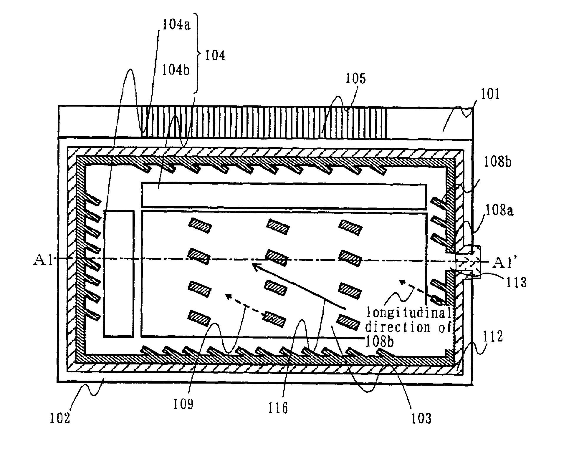
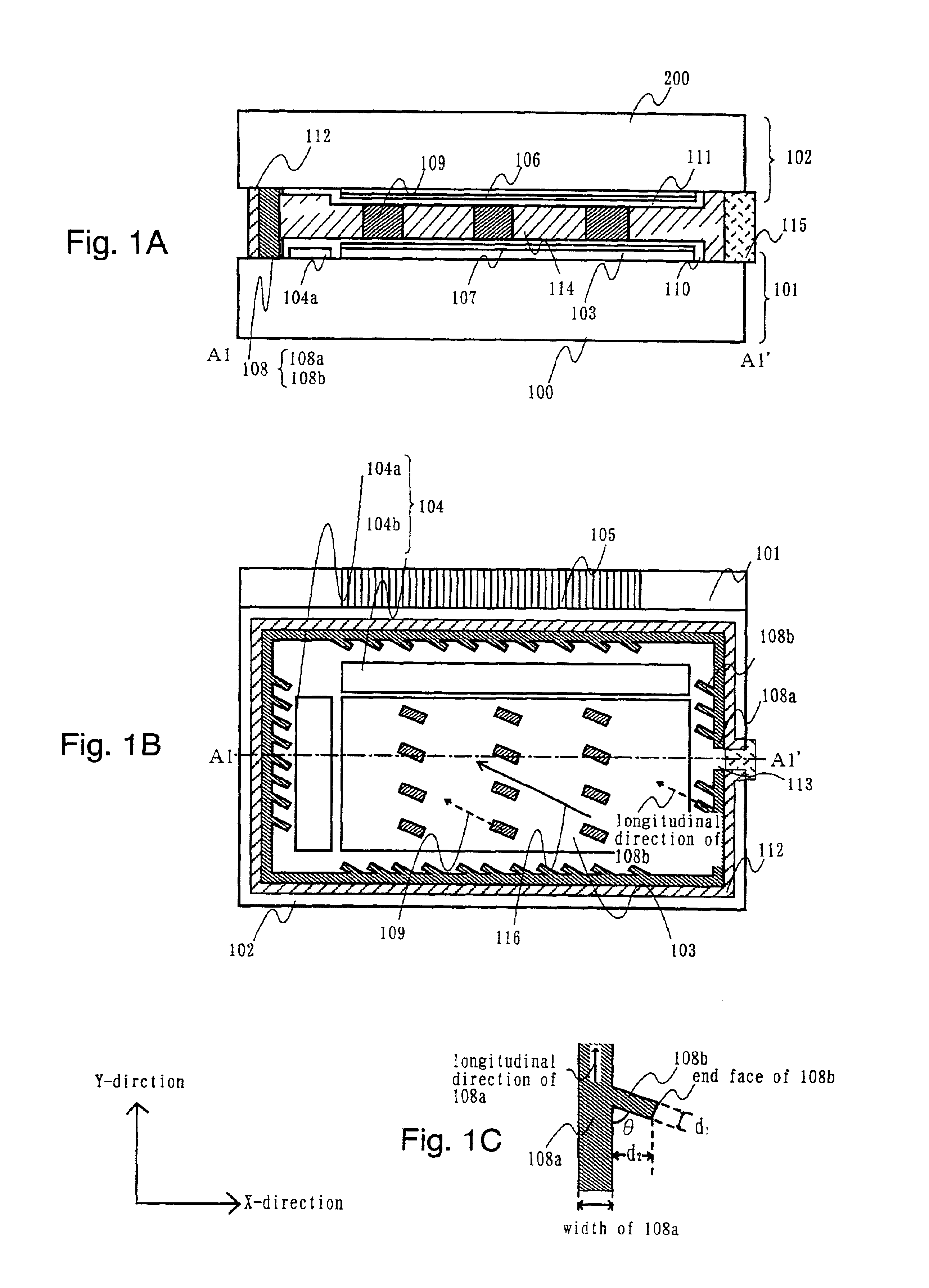
In Embodiment 1, the rubbing treatment has been done as the orienting treatment. In the present embodiment, however, here will be described a method of performing the orienting treatment by forming concaves in the electrode.
embodiment 1
In Embodiment 1, the homogeneous orientation of the liquid crystals is realized with the orientation film oriented, the orientation regulating member and the spacer. In the present embodiment, however, the homogeneous orientation of the liquid crystals can be realized with concaves in the pixel electrode and the orientation regulating member.
Here, the remaining manufacture steps have already been described in Embodiment 1. Therefore, the detailed manufacture steps will be referred to those of Embodiment 1, the description of which will be omitted.
A pixel electrode is formed in the display pixel portion by forming a transparent conductive film (having a film thickness of 110 nm) all over the active matrix substrate and by patterning it using a photomask. The pixel electrode can be formed by a sputtering method or vacuum evaporation method using indium oxide (In2O3) or an alloy of indium oxide-tin oxide (In2O3—SnO2: ITO film). This material is etched with a solution of hydrochloric ac...
embodiment 3
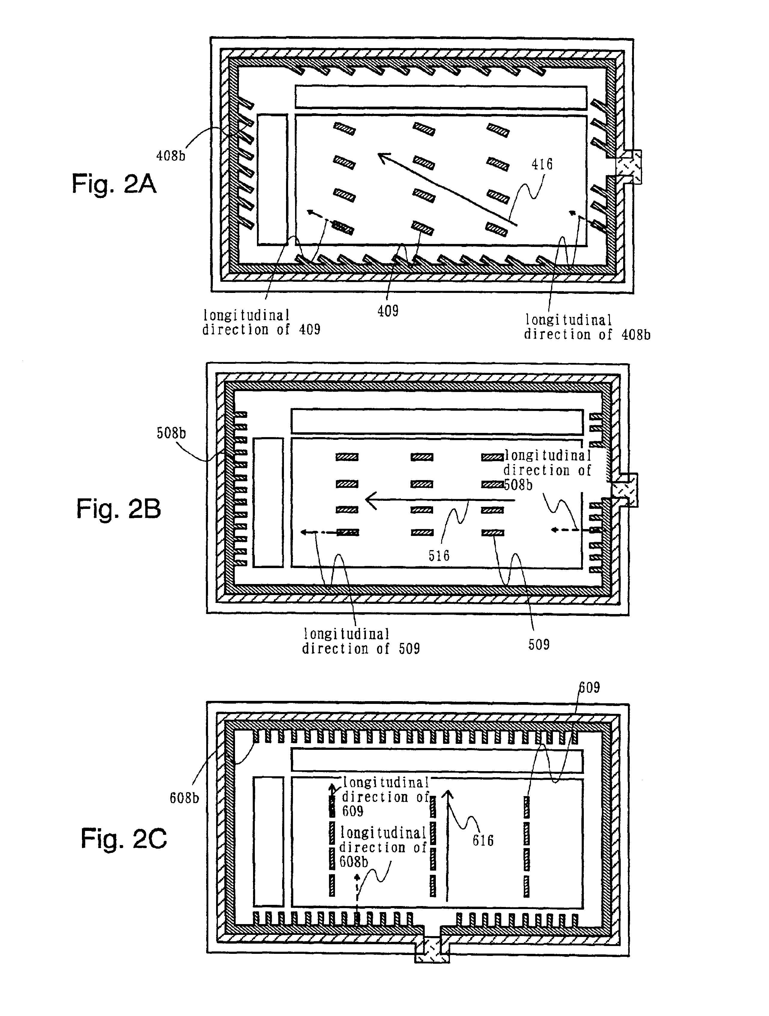
[Embodiment 3]
Where the seal member is to be formed on the opposed substrate, it is desired to form the orientation regulating member on the opposed substrate. The present embodiment is exemplified by forming the orientation regulating member on the opposed substrate.
By the known method, there are formed over a substrate 201: a shielding film 202; a color layer 203 composed of a color layer 203a having a red pattern, a color layer 203b having a green pattern and a color layer 203c having a blue pattern; and a flattening film 204.
Next, a transparent conductive film is applied by a method similar to that used in Embodiment 1, to form the opposed electrode 106. There is obtained an opposed substrate, as shown in FIG. 4A.
Next, the orientation regulating member (although not shown) and the spacer (although not shown) are patterned to a predetermined by a photolithographic method similar to that used in Embodiment 1.
An orientation film is applied to the opposed substrate having the orient...
PUM
| Property | Measurement | Unit |
|---|---|---|
| angle | aaaaa | aaaaa |
| angle | aaaaa | aaaaa |
| width | aaaaa | aaaaa |
Abstract
Description
Claims
Application Information