EEPROM cell having a floating-gate transistor within a cell well and a process for fabricating the memory cell

a floating-gate transistor and memory cell technology, applied in the field of nonvolatile memory devices, can solve the problems of high voltage and low voltage transistors, particularly difficult to fabricate eeprom devices,

Inactive Publication Date: 2005-01-11
LATTICE SEMICON CORP
View PDF6 Cites 8 Cited by
  • Summary
  • Abstract
  • Description
  • Claims
  • Application Information

AI Technical Summary

Problems solved by technology

Electrically-erasable-read-only-memory (EEPROM) devices are particularly difficult to fabricate at high packing density because of the relatively large

Method used


Image

  • EEPROM cell having a floating-gate transistor within a cell well and a process for fabricating the memory cell
  • EEPROM cell having a floating-gate transistor within a cell well and a process for fabricating the memory cell
  • EEPROM cell having a floating-gate transistor within a cell well and a process for fabricating the memory cell

Examples


Embodiment Construction

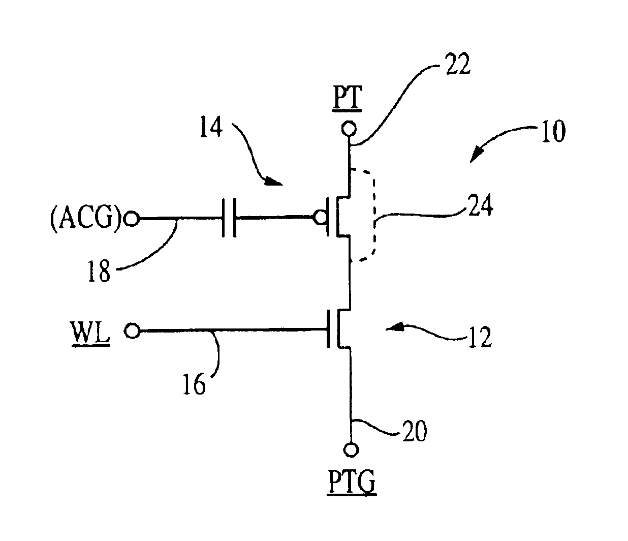
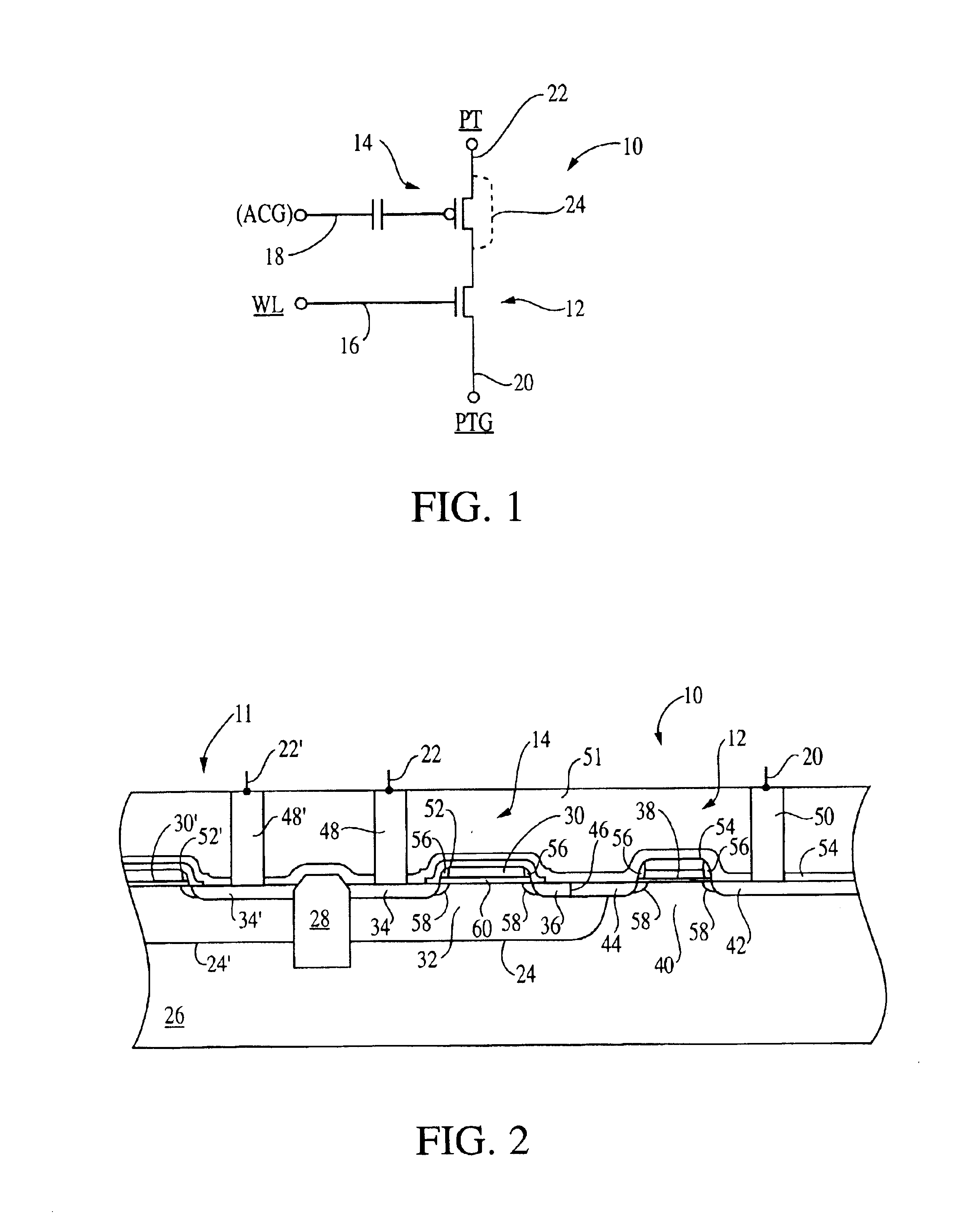
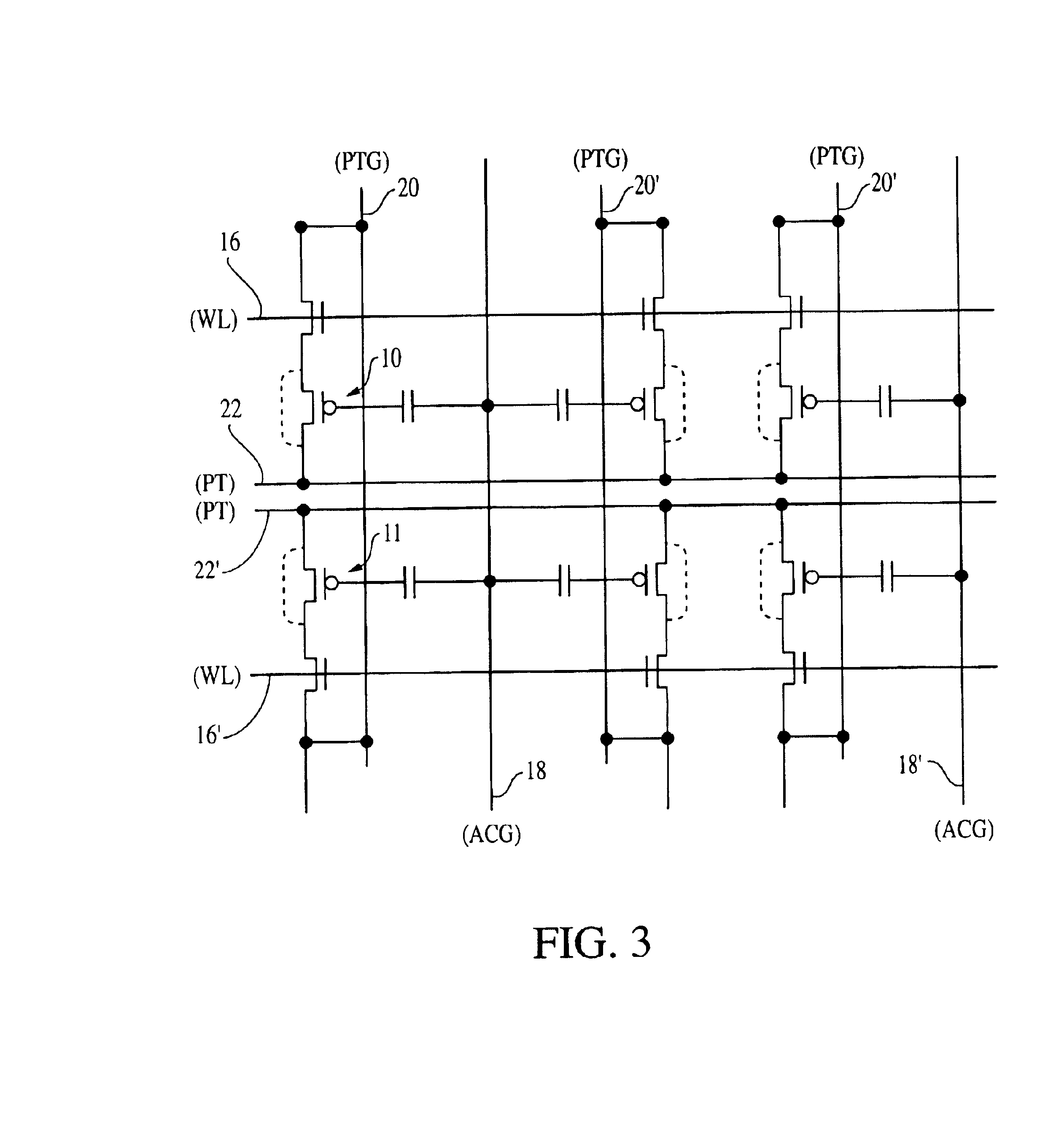
FIG. 1 illustrates a schematic circuit diagram of a two-transistor memory cell 10 arranged in accordance with one embodiment of the invention. The two-transistor memory cell includes a write transistor 12 and floating-gate transistor 14. A word line 16 is electrically coupled to the gate electrode of write transistor 12. A control-gate region 18 is capacitively coupled to the gate electrode of floating-gate transistor 14. A bit line 20 is electrically coupled to an electrode region of write transistor 12 and a sense line 22 is electrically coupled to an electrode region of floating-gate transistor 14. In accordance with the invention, the electrode regions and the channel region of floating-gate electrode 14 are formed in a cell well region 24.

FIG. 2 illustrates, in cross-section, memory cell 10 and a portion of an adjacent memory cell 11. Cell well region 24 resides in a semiconductor substrate 26. The active regions of memory cells 10 and 11 are electrically isolated from each oth...


PUM


Abstract

An EEPROM memory device includes a substrate of a first conductivity type having a cell well region of a second conductivity type therein. A floating-gate transistor of the first conductivity type resides in the cell well region and includes a first region separated from a second region by a channel region. A write transistor of the second conductivity type resides in the substrate and includes a first region separated from a second region by a channel region. The second region partially extends into the cell well region and forms a p-n junction with the second region of the floating-gate transistor. The process for fabricating the EEPROM device includes forming the cell well region in the substrate by creating a retrograde doping profile. In operation, the EEPROM device transfers electrons between the cell well region and the floating-gate electrode during both programming and erasing operations.

Description

TECHNICAL FIELDThe present invention relates, generally, to non-volatile memory devices and to methods of fabrication and, more particularly, to EEPROM cells and to methods for their fabrication.BACKGROUNDThe trend in semiconductor fabrication technology is toward the construction of smaller and smaller devices. As the feature size of individual components within a semiconductor device is reduced, the packing density of the devices can be increased. Accordingly, in addition to fabricating devices having reduced feature sizes, cell architecture plays an important role in achieving high packing densities. Electrically-erasable-read-only-memory (EEPROM) devices are particularly difficult to fabricate at high packing density because of the relatively large capacitive coupling necessary to program and erase the device. Further, EEPROM cells require high voltage and low voltage transistors for their operation. These factors lead to relatively large cell size and accompanying smaller stora...

Claims


Application Information

Patent Timeline
IPC IPC(8): G11C16/04H01L21/8247H01L27/115
CPCG11C16/0433H01L27/11558H01L27/11521H01L27/115H10B69/00H10B41/30H10B41/60
Inventor HU, YONGZHONG
Owner LATTICE SEMICON CORP
Why Eureka
Try Eureka