Display panel with bypassing lines

a technology of bypassing lines and display panels, applied in the field of display panels, can solve the problems of increasing resistance and loading, and unable to effectively operate the signal intensity of decreasing signal intensity, and achieve the effect of reducing resistan

Inactive Publication Date: 2005-01-18
AU OPTRONICS CORP
View PDF1 Cites 14 Cited by
  • Summary
  • Abstract
  • Description
  • Claims
  • Application Information

AI Technical Summary

Benefits of technology

An objective of the present invention is to provide a display panel with flexible printed circuit boards con

Problems solved by technology

However, when the size of display panel desired is unceasingly increased, both the number of the gate driver IC chips 20 and the length of the WOA lines 22 are raised so as to cause the resistance and the loading too high.
And because each gate driver IC chip 20 also possesses considerable resistance, the decreasing signal inten

Method used


Image

  • Display panel with bypassing lines
  • Display panel with bypassing lines
  • Display panel with bypassing lines

Examples


Embodiment Construction

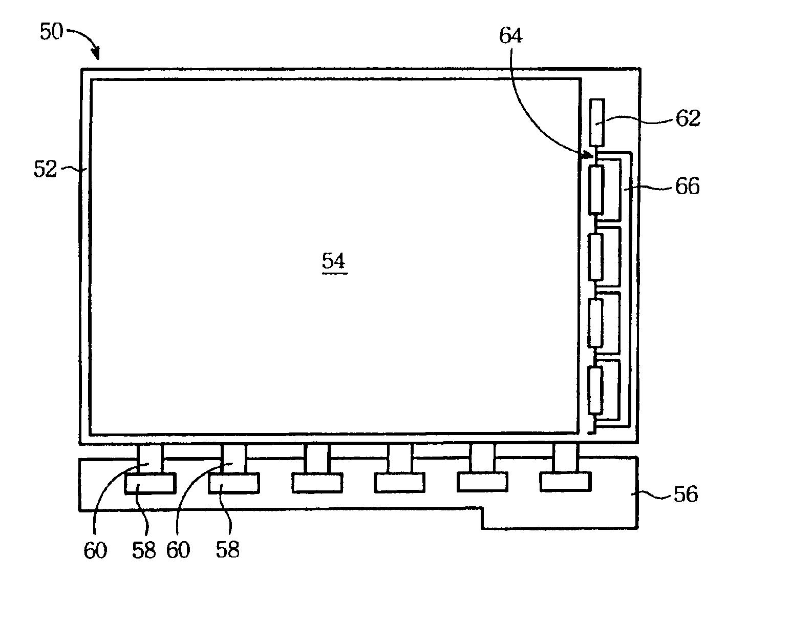
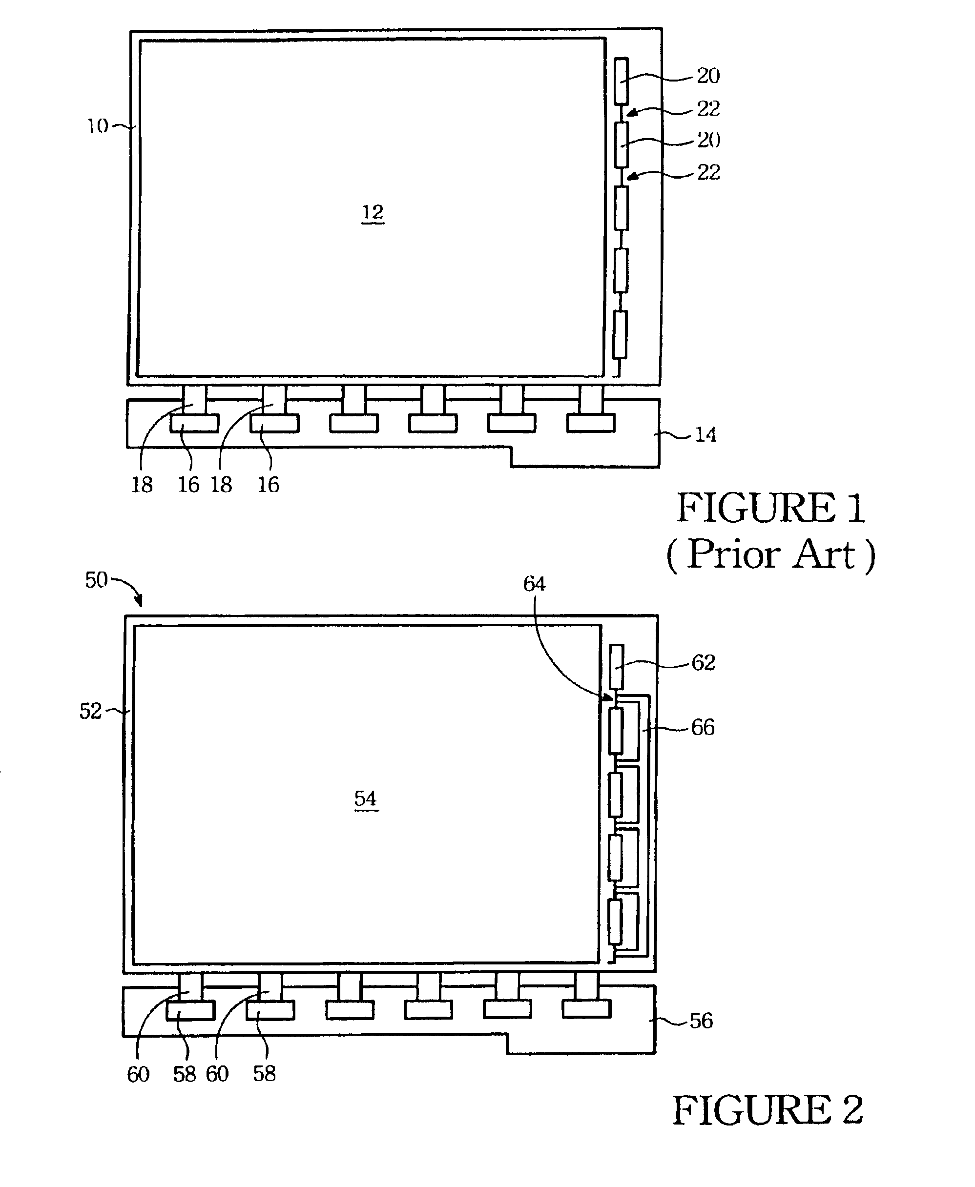
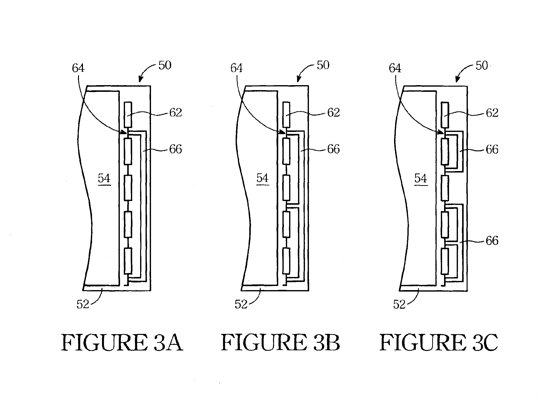
Please refer to FIG. 2, the manner of applying a flexible printed circuits board to provide signals bypassing paths according to the present invention is illustrated. As above-mentioned, a liquid crystal display panel 50 comprises a lower glass substrate 52, an upper glass substrate 54, and a liquid crystal molecules layer placed in between these two glass substrates 52&54. In generally, on the lower glass substrate 52 a large number of TFTs, scan lines and data lines in a crisscross pattern are fabricated to constitute the pixel array. And beneath the upper glass substrate 54 a color filter (CF) film is fabricated so as to produce desired images via the inserted liquid crystal molecules layer after associating with the lower glass substrate 52.

Besides, for effectively operating the TFTs in the LCD panel 50, beneath the LCD panel 50 a printed circuits board (PCB) 56 is connected for transferring driving signals to the LCD panel 50 via a timing control chip (not shown) and source dri...


PUM


Abstract

A display panel comprises the following elements. A pixel array arranged by a plurality of pixel devices is applied for producing images according to input signals. A plurality of COG chips are fabricated on a peripheral region of the display panel and connected in series wherein the COG chips can convey the input signals to the pixel array for driving selected the pixel devices. A plurality of WOA lines are defined on the display panel for connecting the COG chips in series to transfer the input signals. And a first bypassing bus is fabricated aside the COG chips and connected separately to two different WOA lines for connecting with at least one the COG chip in parallel so as to bypass the input signals.

Description

FIELD OF THE INVENTIONThe present invention relates to an approach to promote the electrical connecting performance of liquid crystal displays by using flexible printed circuit boards (FPCs) and, more specifically, to a design of disposing flexible printed circuit boards onto display panels to overcome the high resistance of chip on glass (COG) and wire on array (WOA).BACKGROUND OF THE INVENTIONWith rapid advancement of the fabrication technology of a thin film transistor liquid crystal display (TFT-LCD), the LCD is largely applied in various electronic products such as a Personal Digital Assistant (PDA) device, a laptop, a digital camera, a video camera, and a mobile phone due to the fact it has advantages of smaller size, less weight, lower power consumption and low radiation. Moreover, the quality of the LCD is ceaselessly improved and the price thereof is continuously decreased since manufacturers aggressively invest in research & development and employ large-scale fabricating e...

Claims


Application Information

Patent Timeline
IPC IPC(8): G02F1/13
CPCG02F1/13452Y10S257/92
Inventor CHEN, SHAN-TEWANG, CHIH-SUNGYANG, CHIN-CHENSU, SHENG-LUNLIN, KE-FENG
Owner AU OPTRONICS CORP
Why Eureka
Try Eureka