Method to reduce junction leakage current in strained silicon on silicon-germanium devices

a technology of strained silicon and junction leakage current, which is applied in the manufacturing of semiconductor/solid-state devices, basic electric elements, electric devices, etc., can solve the problems of strained silicon, unviable further developments in conventional silicon technology, and inability to meet the needs of junction leakage current reduction, etc., and achieve the effect of reducing the junction area

Inactive Publication Date: 2005-01-25
AGENCY FOR SCI TECH & RES
View PDF15 Cites 28 Cited by
  • Summary
  • Abstract
  • Description
  • Claims
  • Application Information

AI Technical Summary

Benefits of technology

In accordance with these objectives, a method is described to fabricate an MOSFET device in strained-silicon on SiGe layer which is deposited on a silicon substrate. Shallow isolation trenches are first formed in the strained-silicon / SiGe stack. Next, wet oxidation is done at 700° C. so that SiGe is oxidized selectively with respect to strained or bulk silicon to form a liner oxide on the shallow trench surfaces. An encroachment of about 0.2 μm is achieved under these conditions at the interface between source / drain and shallow trench. The trenches are then filled with CVD oxide, chemically mechanically polished, and the oxide / nitride mask stripped. The MOS transistor is then fabricated using standard steps of gate oxidation of the strained-silicon, poly-silicon gate deposition, patterning the gate, ion implanting / annealing the source / drain regions and the poly-silicon gate. Because of encroachment achieved during wet oxidation, the junction area is reduced because of which the n+ / p junction leakage is correspondingly reduced.

Problems solved by technology

However, economic and physical constraints are rendering further developments to conventional silicon technology unviable.
With up to 4.2% lattice mismatch between relaxed Si and SiGe, silicon lattice when epitaxially deposited on relaxed SiGe gets stretched resulting in strained silicon.
The SS technology is not without its challenges, being quite new to the business.
In addition, the challenges faced by bulk silicon such as short channel effects, device isolation, CMOS integration issues are also applicable to strained silicon.
One limitation of a device featuring a p-n junction on strained Si / SiGe substrate is the higher junction leakage current compared to bulk Si, associated with the lower band gap of SiGe.
As MOSFET features p-n junction in the form of source-to-substrate and drain-to-substrate, the leakage current problem can be dominant during reverse biasing of the drain junction.

Method used


Image

  • Method to reduce junction leakage current in strained silicon on silicon-germanium devices
  • Method to reduce junction leakage current in strained silicon on silicon-germanium devices
  • Method to reduce junction leakage current in strained silicon on silicon-germanium devices

Examples


Embodiment Construction

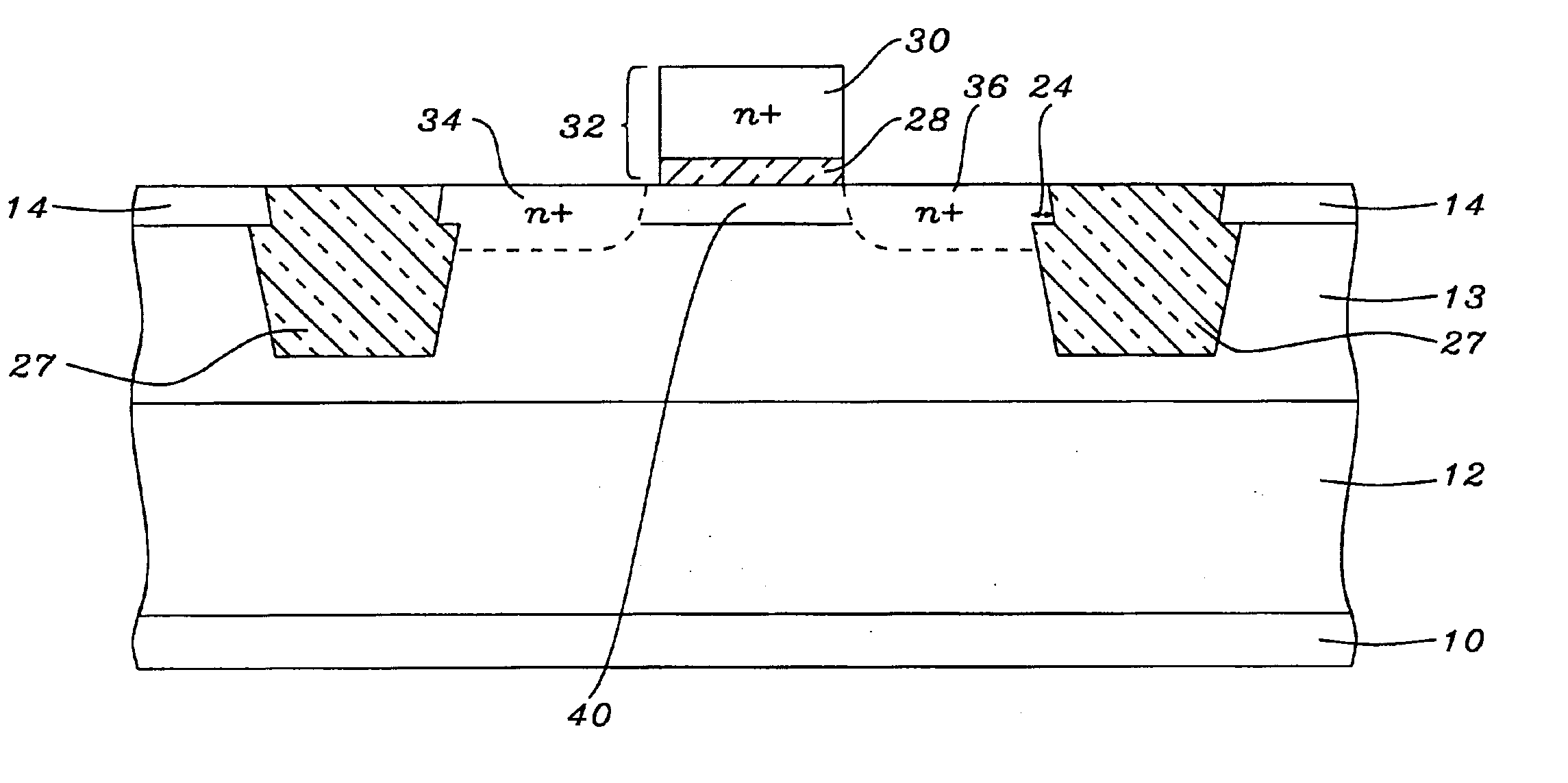
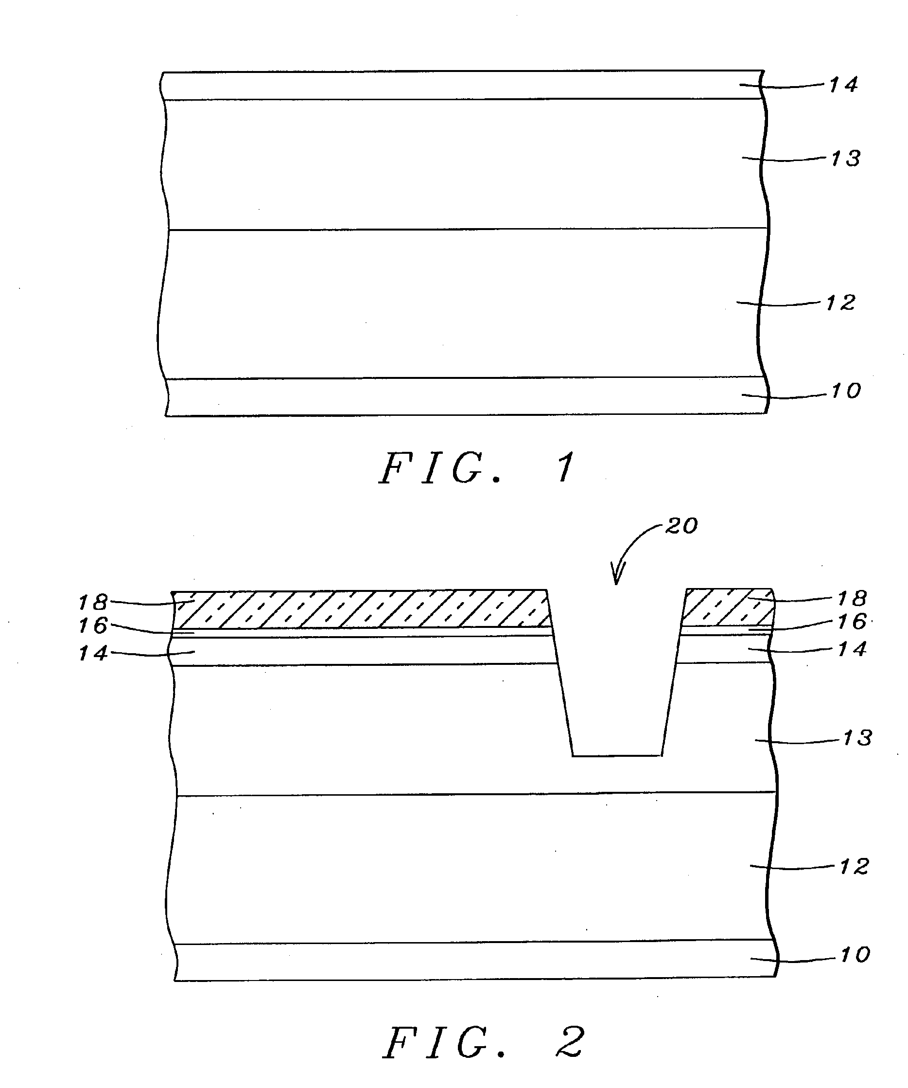
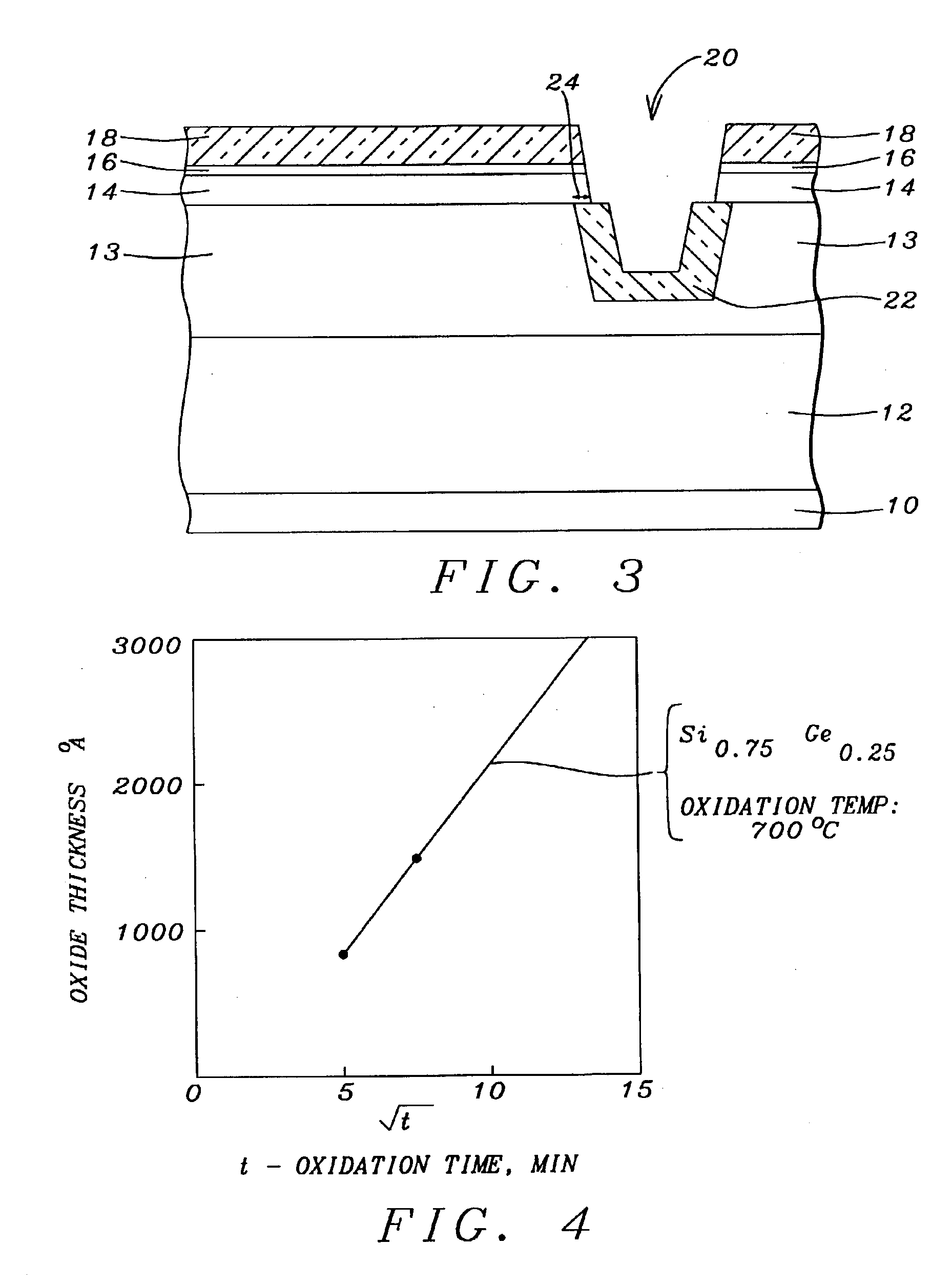
Strained-silicon MOSFETs are formed on a composite substrate, shown in FIG. 1, consisting of a bulk silicon substrate 10, graded composition silicon germanium buffer layer 12, uniform composition SiGe buffer layer 13, and a thin layer of strained silicon layer 14 heteroepitaxially deposited over SiGe layer. The deposition processes known in prior art are used for depositing said SiGe and thin Si layers. Said graded composition SiGe buffer layer, p-type in one embodiment, is approximately about 1 μm-4 μm thick, uniform composition buffer SiGe layer 13 is approximately about 0.5 μm-2 μm thick, and said top silicon layer 14 is approximately 50-400°A thick. In the graded SiGe buffer layer, Ge composition is graded in that there is a higher concentration of Germanium (Ge) atoms near the top. Maximum germanium concentration in the graded layer can vary from 0-40%. Said uniform composition SiGe buffer layer (composition is the same as the maximum value of the graded layer) being thicker, l...


PUM

PropertyMeasurementUnit
thicknessaaaaaaaaaa
thicknessaaaaaaaaaa
thicknessaaaaaaaaaa

Abstract

A MOSFET device in strained silicon-on-SiGe and a method of forming the device are described. The said device achieves reduced junction leakage due to the lower band-gap values of SiGe. The method consists of forming isolation trenches in a composite strained-Si/SiGe substrate and growing a liner oxide by wet oxidation such that oxidation is selective to SiGe only, with negligible oxidation of silicon surfaces. Selective oxidation results in oxide encroachment under strained-Si, thereby reducing the junction area after device fabrication is completed. Reduced junction area leads to reduced n+/p or p+/n junction leakage current.

Description

BACKGROUND OF THE INVENTION(1) Field of the InventionThe present invention relates generally to a silicon on silicon-germanium (SiGe) device and particularly to a method for reducing junction leakage current in an MOS device formed in strained silicon on SiGe.(2) Description of the Prior ArtContinuous demand for improved performance in the electronics industry has been possible as a result of materials, equipment, and process advances related to silicon technology. However, economic and physical constraints are rendering further developments to conventional silicon technology unviable. To date, the performance of a semiconductor device has improved its performance by miniaturizing the dimensions and by increasing scale of integration. There has been therefore, in the last five years, a lot of discussion in trade journals on a new technology, strained-silicon transistors, that has potential use in the next CMOS (complimentary CMOS) generations. The strained-silicon (SS) transistor is...

Claims


Application Information

Patent Timeline
Patent Type & Authority Patents(United States)
IPC IPC(8): H01L29/02H01L29/10H01L21/20H01L21/762
CPCH01L29/1054H01L21/76232H01L21/0245H01L21/02505H01L21/0251H01L21/02664H01L21/02532
Inventor BALASUBRAMANIAN, NARAYANANHAMMOND, RICHARD
Owner AGENCY FOR SCI TECH & RES
Why Eureka
Try Eureka