Semiconductor device

Inactive Publication Date: 2005-01-25
OUME ELECTRONICS CO LTD +1
View PDF28 Cites 98 Cited by
  • Summary
  • Abstract
  • Description
  • Claims
  • Application Information

AI Technical Summary

Benefits of technology

[0014]An object of the present invention is to provide a semiconductor device capable of mounting passive elements on a

Problems solved by technology

However, the formation of these passive elements necessitates a relatively large area, with the result that, if these passive elements are to be formed in the circuit element-forming region DA, the chip area is unavoidably increased.
If the chip area is increased in the semiconductor device 10 of the CSP structu

Method used


Image

  • Semiconductor device
  • Semiconductor device
  • Semiconductor device

Examples


fourth embodiment

[0057]FIG. 35A is a cross sectional view showing a third connection mode of an inductance element according to the present invention;

[0058]FIG. 35B is an equivalent circuit diagram corresponding to the connection mode of the inductance element shown in FIG. 35A;

[0059]FIG. 36A is a cross sectional view showing a fourth connection mode of an inductance element according to the fourth embodiment of the present invention;

[0060]FIG. 36B is an equivalent circuit diagram corresponding to the connection mode of the inductance element shown in FIG. 36A;

fifth embodiment

[0061]FIG. 37 is a cross sectional view showing the construction of a semiconductor device according to the present invention;

sixth embodiment

[0062]FIG. 38 is a cross sectional view showing the construction of a semiconductor device according to the present invention;

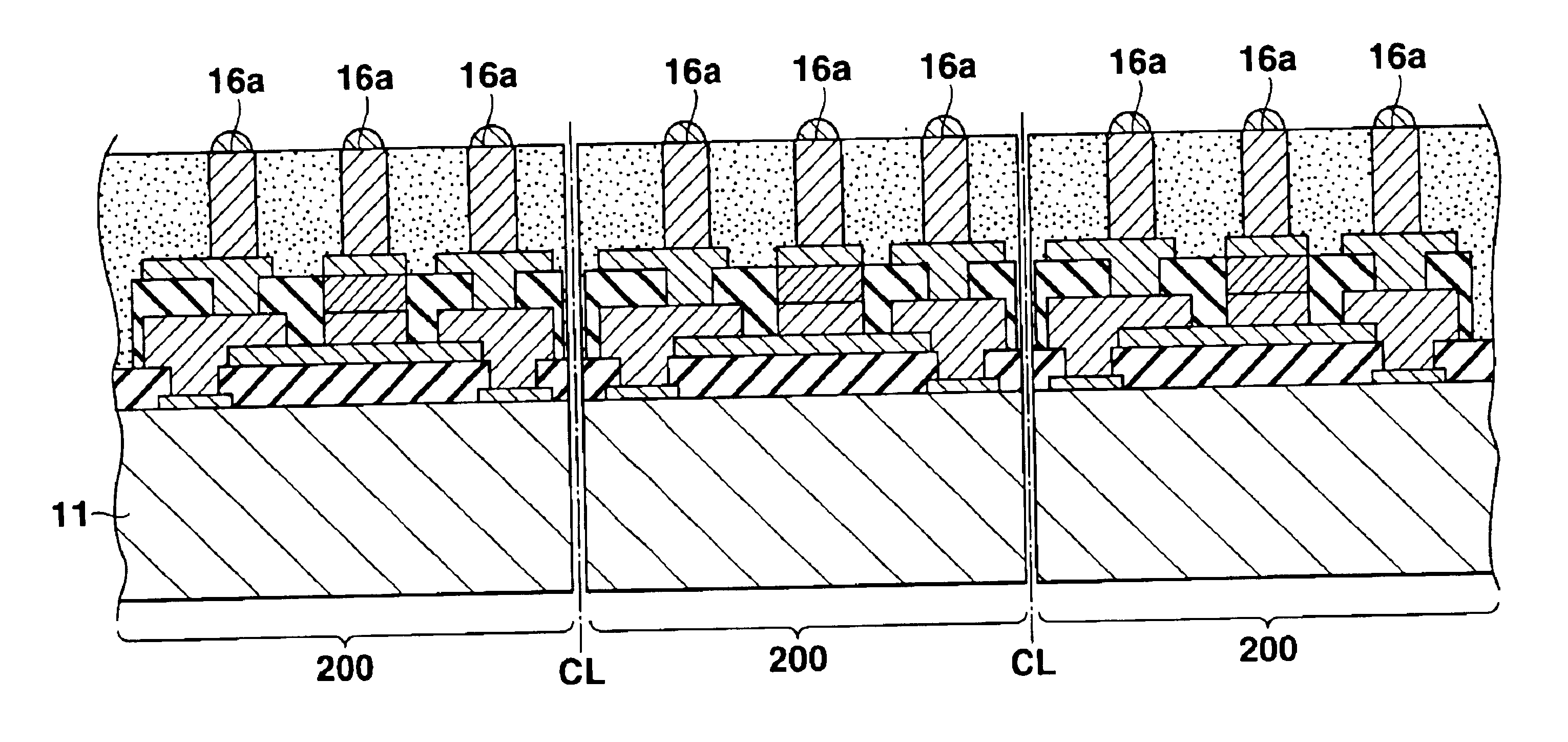
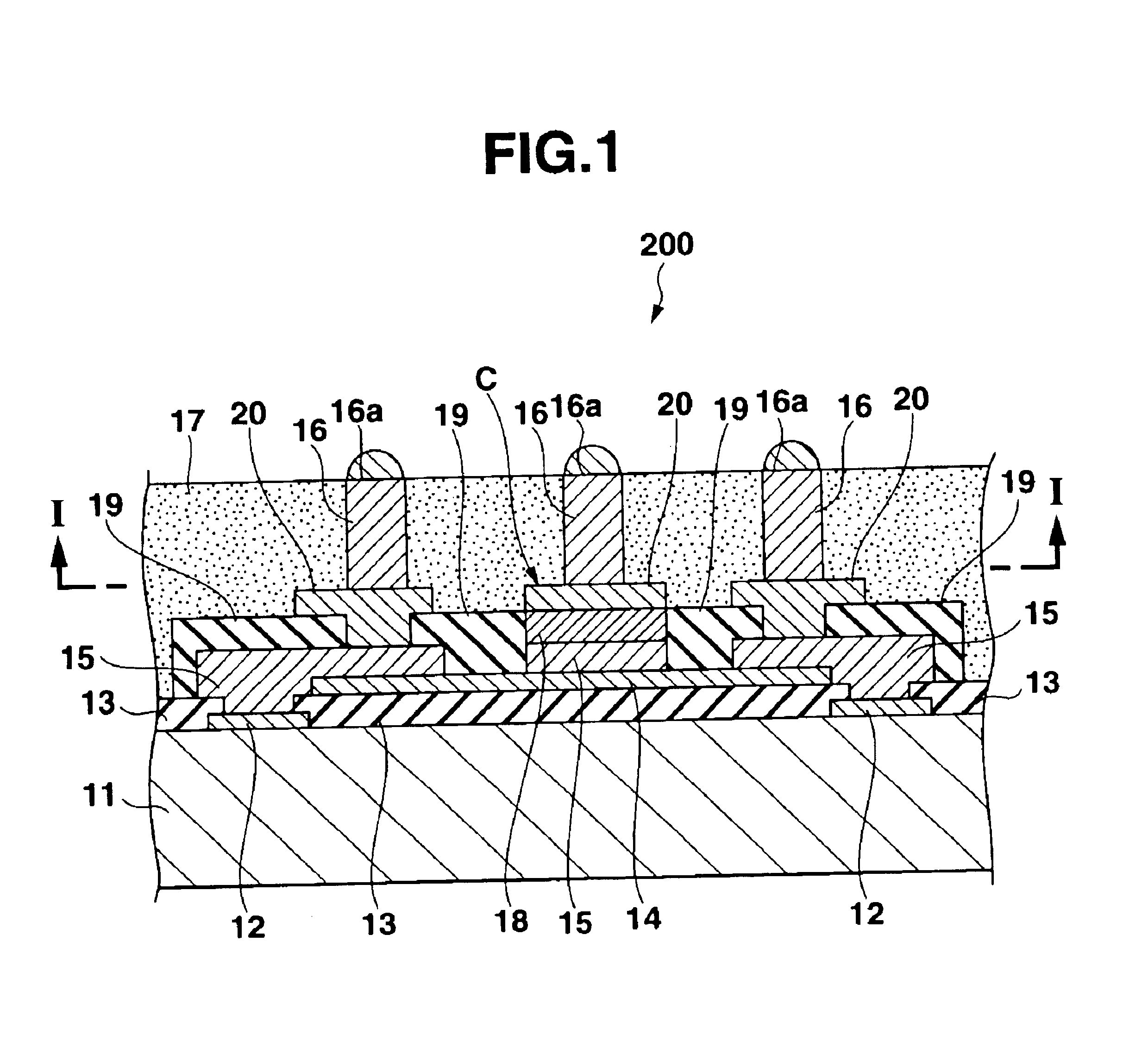
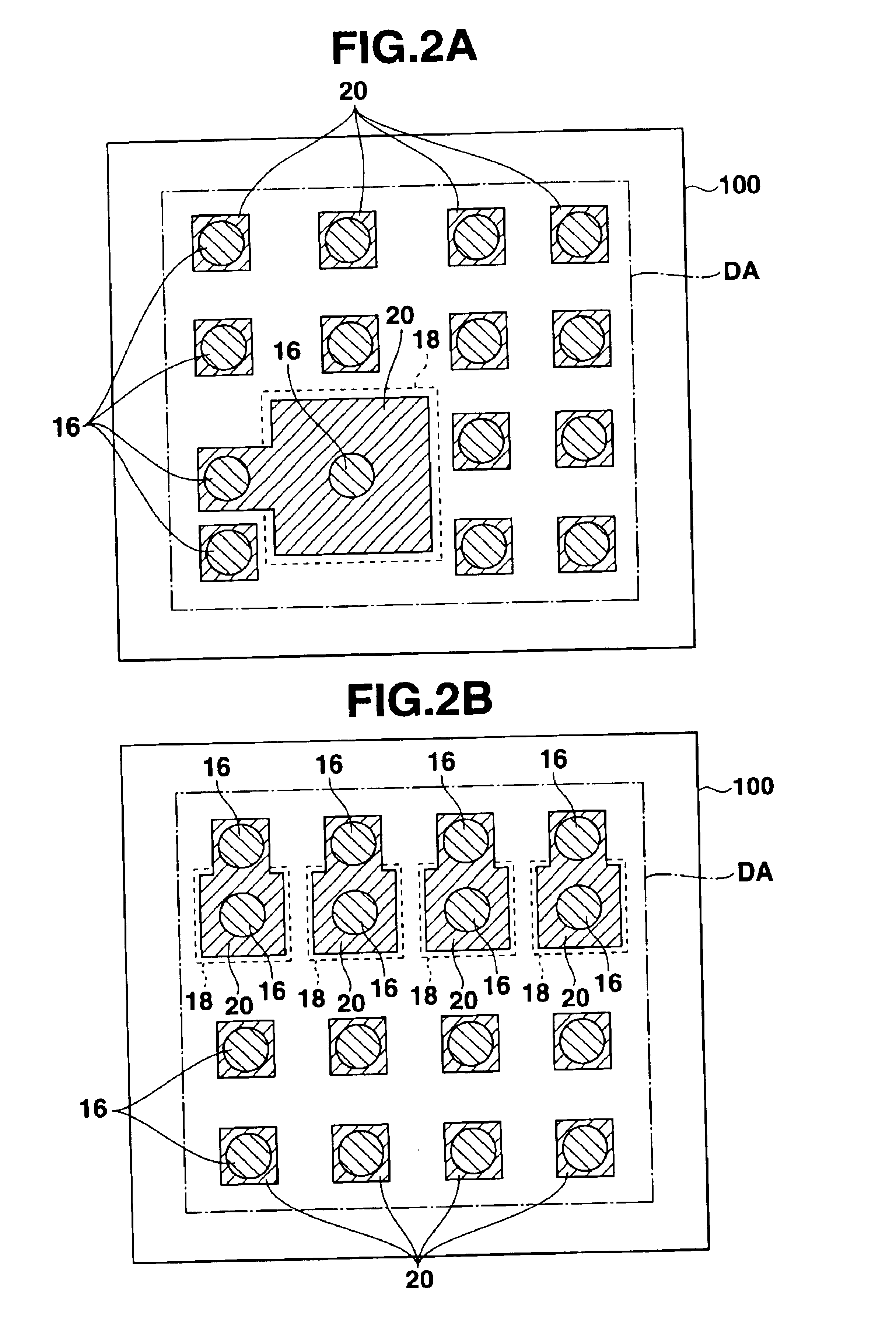
[0063]FIG. 39 is a cross sectional view showing the construction of a semiconductor device having the passive elements of the various embodiments of the present invention arranged therein;

[0064]FIG. 40 is a cross sectional view showing the construction of a conventional semiconductor device; and

[0065]FIG. 41 is a cross sectional view of the conventional semiconductor device along the line V—V shown in FIG. 40.

DETAILED DESCRIPTION OF THE INVENTION

[0066]The construction and the manufacturing method of a semiconductor device of the present invention will now be described in detail with reference to the accompanying drawings showing preferred embodiments of the present invention.

[0067]


PUM


Abstract

A thin film passive element includes at least one of a capacitance element having a plurality of conductive layers and a dielectric material layer and an inductance element formed of a patterned conductive layer is stacked on a circuit element-forming region of a semiconductor substrate provided with a plurality of connection pads and is connected to the circuit element of the circuit element-forming region.

Description

CROSS-REFERENCE TO RELATED APPLICATIONS[0002]This application is based upon and claims the benefit of priority from the prior Japanese Patent Applications No. 2000-243765, filed Aug. 11, 2000; and No. 2000-243783, filed Aug. 11, 2000, the entire contents of both of which are incorporated herein by reference.BACKGROUND OF THE INVENTION[0003]1. Field of the Invention[0004]The present invention relates to a semiconductor device of a CSP (Chip Size Package) structure and a method of manufacturing the same.[0005]2. Description of the Related Art[0006]In recent years, a semiconductor device of a CSP structure, in which the chip size is substantially equal to the package size, has come to be employed for increasing the mounting density of the circuit substrate. FIG. 40 is a cross sectional view exemplifying the construction of a semiconductor device of a CSP structure, and FIG. 41 is a cross sectional view along the line V—V shown in FIG. 40 showing the construction of the semiconductor de...

Claims


Application Information

Patent Timeline
IPC IPC(8): H01L23/28H01L23/31H01L23/522H01L23/52H01L27/08H01L21/02H01L23/48
CPCH01L23/3114H01L23/5223H01L23/5227H01L27/08H01L27/0805H01L28/20H01L2924/0002H01L28/40H01L2924/1423H01L2924/19041H01L2924/00H01L23/48
Inventor TAHARA, IWAOMIHARA, ICHIROAOKI, YUTAKA
Owner OUME ELECTRONICS CO LTD
Why Eureka
Try Eureka