Semiconductor memory having burst transfer function and internal refresh function

a technology of memory and sram, applied in the field of semiconductor memories, can solve the problems of large skew, large skew, and disadvantage of sram in providing large capacity, and achieve the effect of reducing the ratio of address skew to access cycl

Inactive Publication Date: 2005-01-25
SOCIONEXT INC
View PDF13 Cites 22 Cited by
  • Summary
  • Abstract
  • Description
  • Claims
  • Application Information

AI Technical Summary

Benefits of technology

According to another aspect of the semiconductor memory of the present invention, the predetermined time is modified in accordance with the programming of a fuse. Therefore, for example, programming the fuse according to the highest operating frequency as evaluated in a probe test can set the predetermin

Problems solved by technology

However, the SRAMs are disadvantageous in terms of providing large capacities because they require more elements to constitute each one-bit cell than DRAMs.
In general, addresses require large numbers of bits and are supplied not only to the memories but also to other chips in the systems, so that skew is

Method used


Image

  • Semiconductor memory having burst transfer function and internal refresh function
  • Semiconductor memory having burst transfer function and internal refresh function
  • Semiconductor memory having burst transfer function and internal refresh function

Examples


first embodiment

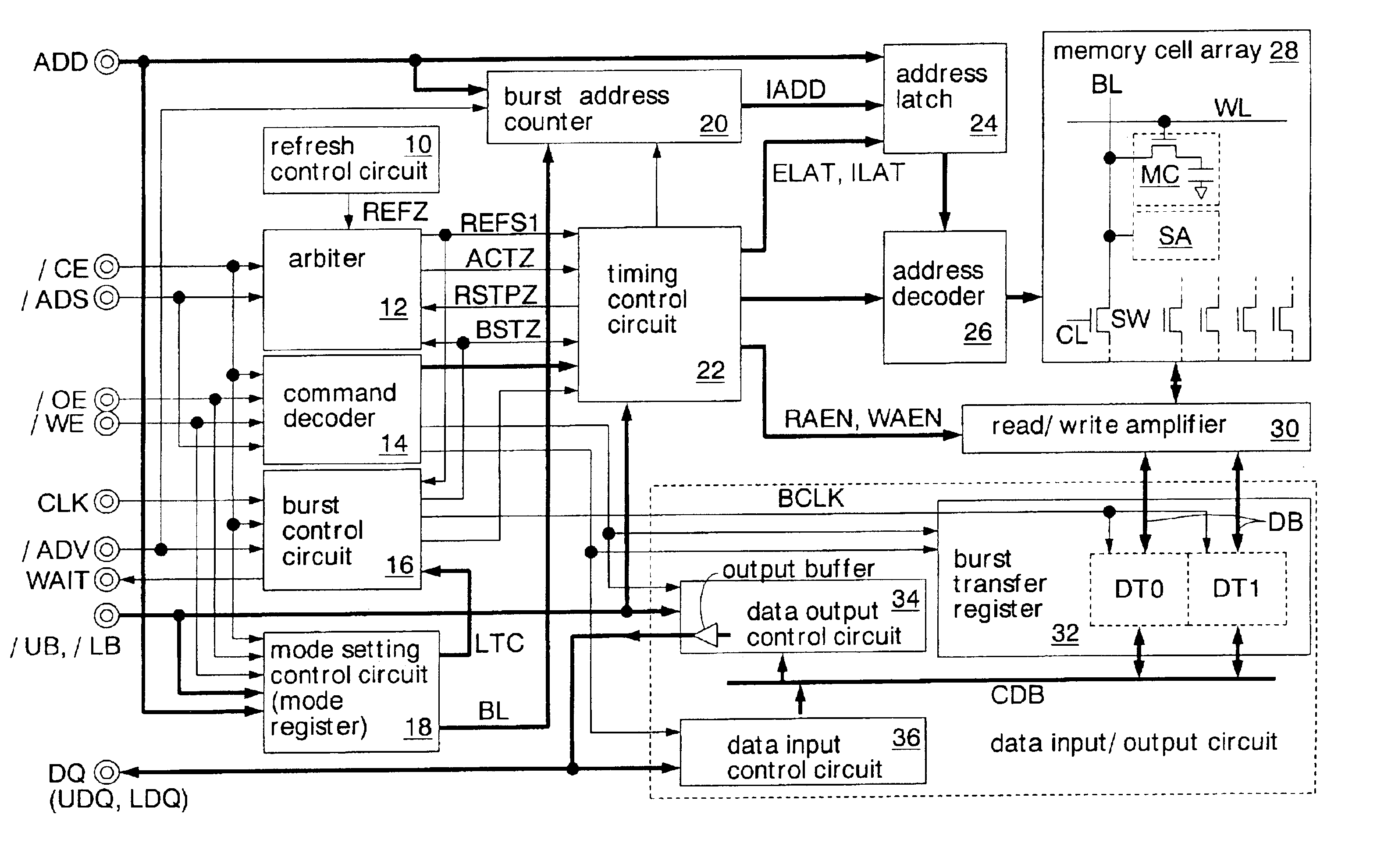
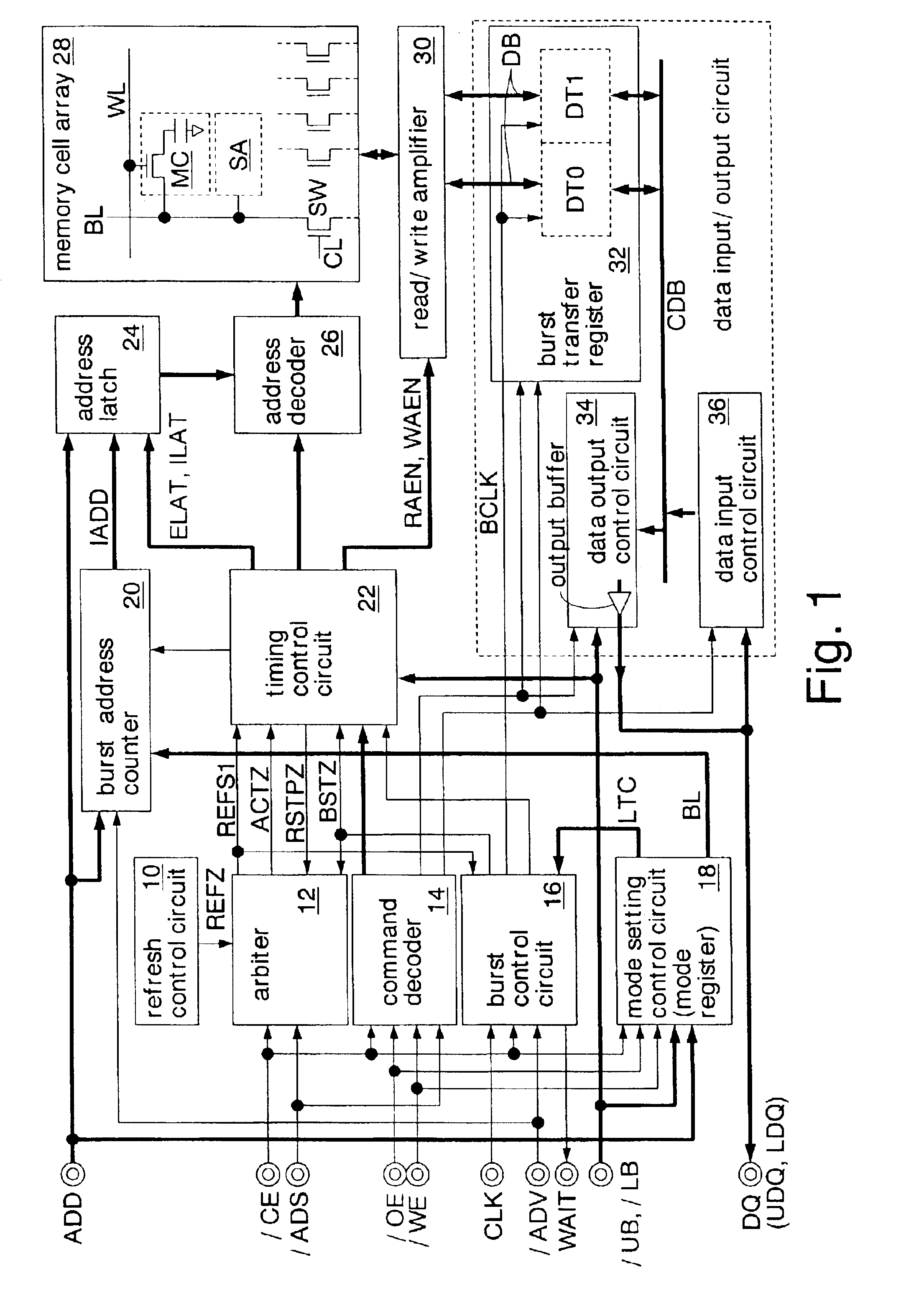
FIG. 1 shows semiconductor memory according to the present invention. In the figure, each of the signal lines shown by thick lines is constituted by a plurality of bits. Double circles shown on the left side of the figure designate external input terminals. The signals identified by designations prefixed with “ / ” represent negative logics, while the signals identified by designations postfixed with “Z” represent positive logics. In the following descriptions, signals may be referred to by using their respective abbreviations; for example, “external clock signal CLK” may be referred to as “CLK signal”, and “chip enable signal / CE” may be referred to as “ / CE signal”.

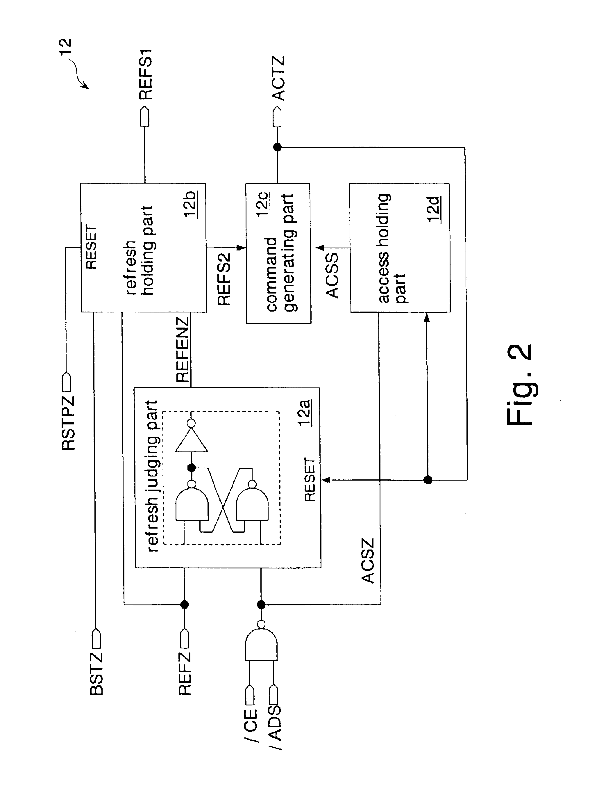
This semiconductor memory is formed as a pseudo SRAM having memory cells as of a DRAM and also having interfaces as of an SRAM. This pseudo SRAM has a refresh control circuit 10, an arbiter 12, a command decoder 14, a burst control circuit 16, a mode setting control circuit 18, a burst address counter 20, a timing control ...

fourth embodiment

FIG. 26 shows the read operation during a burst mode in the pseudo SRAM of the In the present example, the read latency RLTC is set to “2”. The read latency RLTC is the number of clocks from when an output enable signal / OE is activated till when the first read data is outputted.

The burst control circuit 52 starts the outputting of internal clock signals RCLK1 in response to the activation of an output enable signal / OE during the read operation (FIG. 26(a)). The basic timings of the following operations during the burst read operation are the same as in the third embodiment (FIG. 20), and hence their descriptions are omitted.

FIG. 27 shows the write operation during a burst mode in the pseudo SRAM of the fourth embodiment. In the present example, the write latency WLTC is set to “2”. The write latency WLTC is the number of clocks from when a write enable signal / WE is activated till when the first write data is inputted.

The burst control circuit 52 starts the outputting of internal...


PUM


Abstract

A refresh control circuit generates a refresh request in a predetermined cycle. A first burst control circuit outputs a predetermined number of strobe signals in accordance with an access command. A burst access operation is executed by an access command. A data input/output circuit successively inputs data to be transferred to a memory cell array or successively outputs data supplied from the memory cell array, in synchronization with the strobe signals. An arbiter determines which of a refresh operation or a burst access operation is to be executed first, when the refresh request and the access command conflict with each other. Therefore, the refresh operation and burst access operation can be sequentially executed without being overlapped. As a result, read data can be outputted at a high speed, and write data can be inputted at a high speed. That is, the data transfer rate can be improved.

Description

BACKGROUND OF THE INVENTION1. Field of the InventionThe present invention relates to semiconductor memories that have volatile memory cells each having a capacitor and that have interfaces as of SRAMs.2. Description of the Related ArtRecently, mobile devices such as cellular phones and the like have advanced service functions, and handling data amount therein has been increasing. Accordingly, there is a growing demand for large capacities of the work memories incorporated in such mobile devices.Conventionally, SRAMs having simple system structure are used as the work memories of such mobile devices. However, the SRAMs are disadvantageous in terms of providing large capacities because they require more elements to constitute each one-bit cell than DRAMs. For this reason, semiconductor memories called pseudo SRAMs have been developed, which have both large capacities as of DRAMs and high usability as of SRAMs.It is expected that mobile devices have further advanced service functions, ...

Claims


Application Information

Patent Timeline
IPC IPC(8): G11C11/406G11C11/403G11C11/407
CPCG11C7/1051G11C7/1063G11C11/4076G11C11/40615G11C11/406G11C11/401
Inventor FUJIOKA, SHINYAOKUYAMA, YOSHIAKI
Owner SOCIONEXT INC
Why Eureka
Try Eureka