Error reduction in semiconductor processes

a technology of semiconductor processes and errors, applied in the field of photolithography, can solve problems such as failure to solve the problem of resolution failure, one or more dies of the wafer being scrapped fast enough to respond. the effect of reducing costs

Inactive Publication Date: 2005-01-25
TEXAS INSTR INC
View PDF6 Cites 3 Cited by
  • Summary
  • Abstract
  • Description
  • Claims
  • Application Information

AI Technical Summary

Benefits of technology

An advantage of the invention is that it provides early detection of a chuck or wafer contamination or other process error and thus eliminates costs associated with processing wafers with die that eventually have to be scrapped as a result of poor resolution caused by the processing error. The invention is particularly useful for detecting repetitive errors that can adversely affect multiple lots of wafers and is fast enough to respond to wafer defects

Problems solved by technology

This often results in resolution failures as the system has difficulty focusing the image in the area of the topographical feature caused by the chucking error.
The local tilt of the wafer surface in the area of the undesired topographical feature can cause misformation of the projected image.
The imaging errors can result in the scrap

Method used


Image

  • Error reduction in semiconductor processes
  • Error reduction in semiconductor processes
  • Error reduction in semiconductor processes

Examples


Embodiment Construction

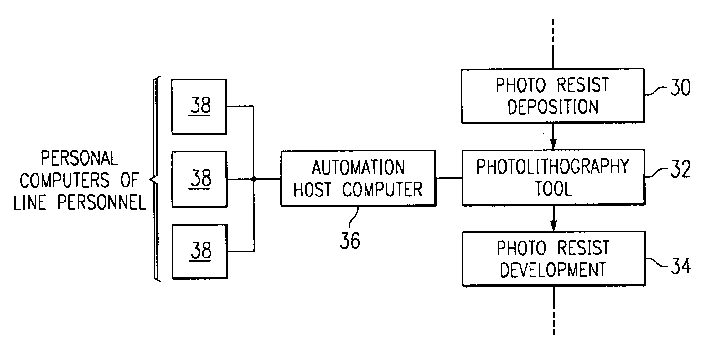
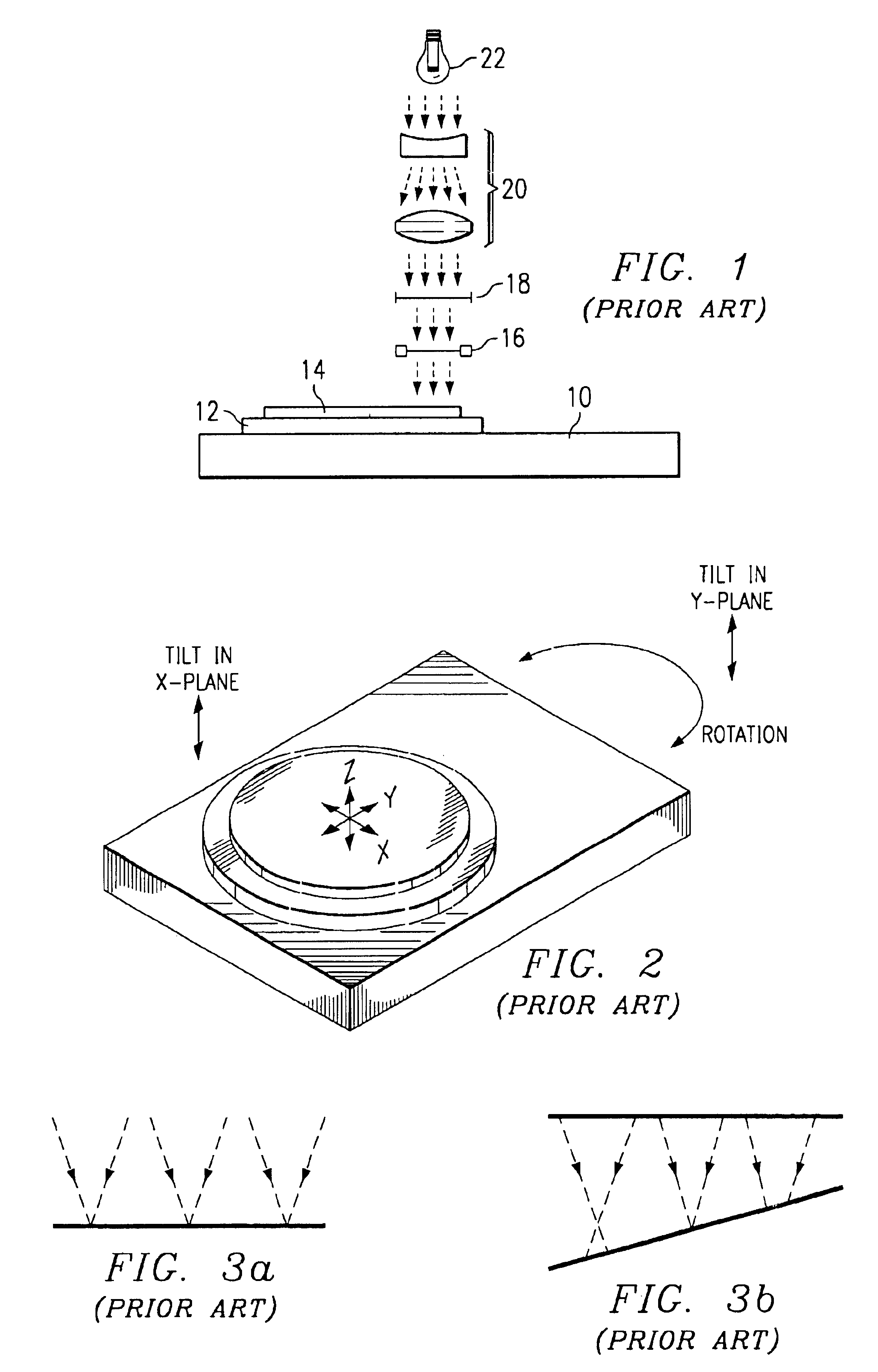
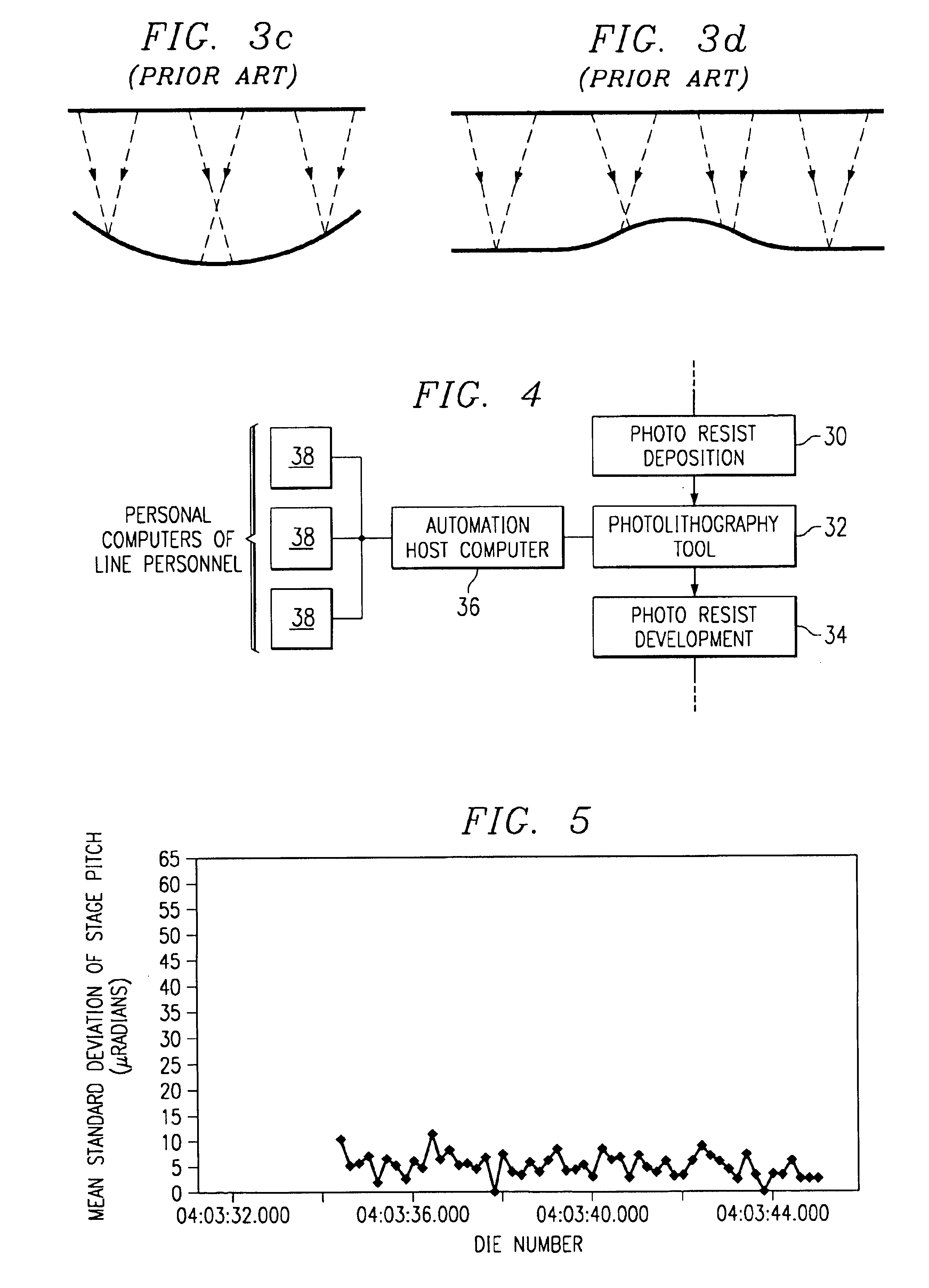
FIG. 4 is a block diagram of a portion of a semiconductor integrated circuit fabrication process. The initial block 30 represents the equipment used to deposit, spin, and bake the photoresist onto a wafer. It is followed by the photolithography tool 32 and then by the equipment 34 dedicated to photoresist development. An automation host computer 36 is coupled to the photolithography tool and is also coupled to the personal computers 38 of relevant line management personnel through a local area network, for example.

In one embodiment of the invention, data recording the movement of the stage as the tool 32 seeks to maintain focus as it steps or scans are used to detect die-to-die, wafer-to-wafer, and lot-to-lot defects or errors that have an adverse effect on yield. The automation host computer 36, which controls the tool, reacts to detection of such problems by generating an alert signal and by taking an action specified in an action look-up table, for example. The severity of the pr...


PUM


Abstract

A photolithography system includes a photolithography tool 32 that includes a stage upon which a semiconductor wafer is mounted. The tool is operable to move the stage to automatically focus a pre-determined image on a surface of the semiconductor wafer. The tool is further operable to log movements of the stage. The system also includes an automation host computer 36 operable to poll the photolithography tool 32 to obtain data reflecting the logged movements of the stage. The automation host computer 36 is further operable to analyze the data and compare the data to pre-determined error conditions. The host computer also takes a pre-determined action, including sending an electronic mail message to the personal computers 38 of relevant line personnel, in the event the data meets the pre-determined error conditions.

Description

BACKGROUND OF THE INVENTIONThis invention is in the field of semiconductor processing, and more particularly in the field of photolithography.In semiconductor processing, photolithography is the process of defining particular features on the surface of a semiconductor wafer. The feature is typically defined with a patterned exposure into a photosensitive material that has been previously deposited on the wafer surface. In a typical photolithographic system, a master pattern image in the form of a photomask or reticle is replicated across the surface of the wafer. The image is typically projected onto the photosensitive material (e.g. photoresist) through a lens system. The quality of the image, and hence the quality and reliability of the resulting feature on the semiconductor surface, is directly related to mechanical parameters such as the spacing and orientation of the lens system relative to the chuck and stage upon which the wafer is placed.Lithography equipment typically inclu...

Claims


Application Information

Patent Timeline
IPC IPC(8): G03F7/20G03F9/00G03F7/207G03F9/02
CPCG03F7/70425G03F9/7026G03F9/7003
Inventor ATKINSON, CHRIS D.MELCHER, KEITH W.GULDI, RICHARD L.
Owner TEXAS INSTR INC
Why Eureka
Try Eureka