Semiconductor device

a technology of semiconductors and devices, applied in the direction of semiconductor devices, basic electric elements, electrical appliances, etc., can solve the problems of increasing production costs, affecting and affecting the performance of the device, so as to achieve the effect of reducing the on-resistance of the devi

Inactive Publication Date: 2005-02-01
KK TOSHIBA
View PDF17 Cites 38 Cited by
  • Summary
  • Abstract
  • Description
  • Claims
  • Application Information

AI Technical Summary

Benefits of technology

According to the present invention, there is provided a semiconductor device comprising:a semiconductor substrate of a first conductivity type;a semiconductor layer of a first conductivity type formed on a first main surface of the semiconductor substrate, the semiconductor layer including a first region for a cell portion and a second region for a terminating portion, the second region being positioned in an outer periphery of the first region, said terminating portion maintaining breakdown voltage by extending a depletion layer to relieve an electric field;junction pairs of semiconductor layers periodically arranged so as to form a line from the first region to the second region in a first direction parallel to the first main surface in the semiconductor layer and having mutually opposite conductivity types of impurities, each of said junction pair being composed of a first impurity diffusion layer of a second conductivity type formed from a surface of the semiconductor layer toward the semico...

Problems solved by technology

However, present technologies have difficulty in forming such a multi RESURF structure by a method other than a so-called multi epitaxial growth technique in which RESURF N layers and P layers are alternatively laminated.
This method considerably increases a production cost due to the repetition of the epitaxial growth step, which eliminates the merits that the ON-resistance of the device can be lowered.
Since quantity imbalance between an N type impurity and a P type impurity may result in lowered breakdown voltage, such variations would be a disadvantage.
Thus, there is no counterpart impurity diffusion layer for charge compensation in the terminating portion, which causes...

Method used


Image

  • Semiconductor device
  • Semiconductor device
  • Semiconductor device

Examples


first embodiment

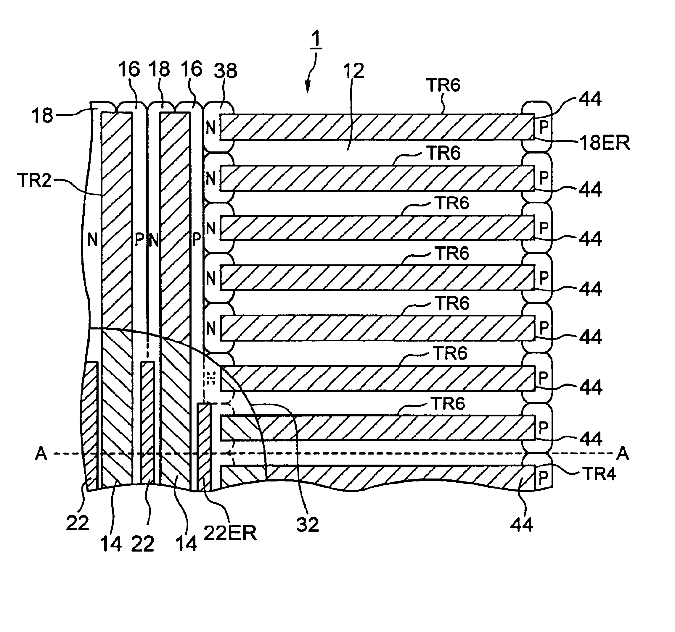
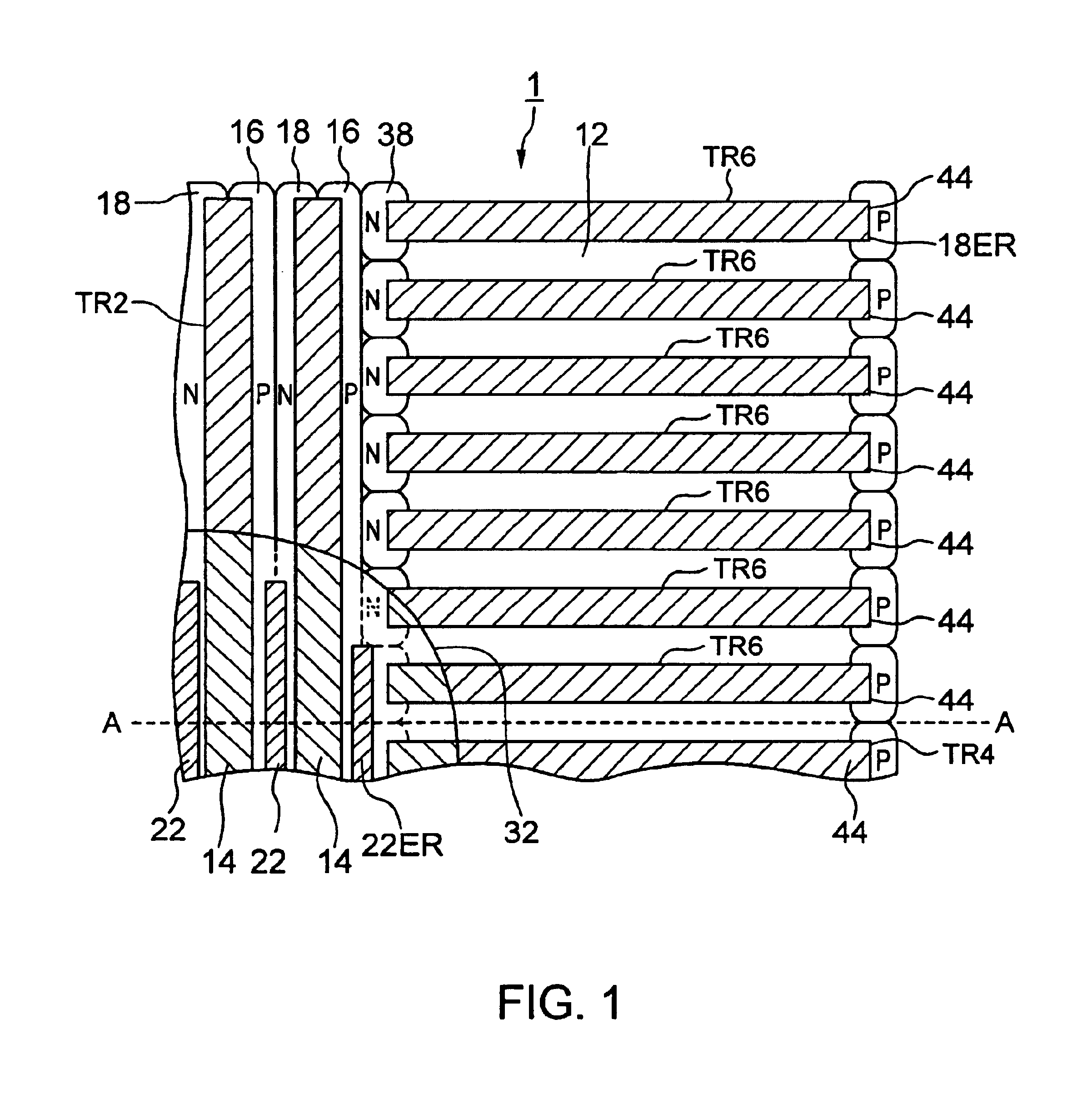
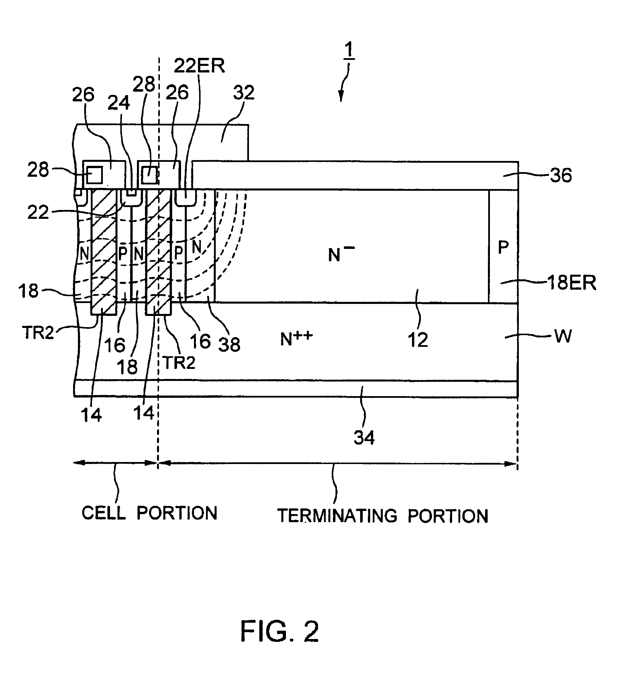
FIG. 1 is a plan view showing one side of a terminating portion in a semiconductor device according to the present invention, and FIG. 2 is a cross-sectional view taken along line A—A in FIG. 1. FIG. 3 is a plan view showing the other side of the terminating portion of the semiconductor device shown in FIG. 1, and FIG. 4 is a cross-sectional view taken along line B—B in FIG. 3. The semiconductor device in this embodiment is characterized in that, an N layer 38 is provided on an outer side of an outermost layer of P layers 16 adjacently thereto in the terminating portion shown in FIGS. 1 and 2, and a P layer 46 is provided on an outer side of an outermost layer of N layers 18 adjacently thereto in the terminating portion shown in FIGS. 3 and 4, whereby a device has the same charge compensation structure even in its terminating portion. The semiconductor device according to this embodiment will be described in more detail below.

A power MOSFET 1 of a vertical trench multi RESURF struct...

second embodiment

Next, the semiconductor device according to the present invention will be described with reference to FIGS. 5 to 8.

FIG. 5 is a plan view showing one side of a terminating portion of the second embodiment of the semiconductor device according to the present invention, and FIG. 6 is a cross-sectional view taken along line C—C of FIG. 5. FIG. 7. is a plan view showing the opposite side of the terminating portion of the semiconductor device shown in FIG. 5, and FIG. 8 is a cross-sectional view taken along line D—D of FIG. 7. The semiconductor device according to this embodiment is characterized in that the combination of the N layer and P layer is successively formed up to the peripheral edge in the terminating portion of the device so as to have the same charge compensation structure throughout the device. A power MOSFET 3 of the vertical trench multi RESURF structure according to this embodiment is formed, in order to obtain such a charge compensation structure, so that trenches TR8 i...


PUM


Abstract

A semiconductor device includes: a semiconductor substrate of a first conductivity type; a semiconductor layer of a first conductivity type formed on a first main surface of the semiconductor substrate, the semiconductor layer including a first region for a cell portion and a second region for a terminating portion, the second region being positioned in an outer periphery of the first region, the terminating portion maintaining breakdown voltage by extending a depletion layer to relieve an electric field; junction pairs of semiconductor layers periodically arranged so as to form a line from the first region to the second region in a first direction parallel to the first main surface in the semiconductor layer and having mutually opposite conductivity types of impurities, each of the junction pair being composed of a first impurity diffusion layer of a second conductivity type formed from a surface of the semiconductor layer toward the semiconductor substrate and a second impurity diffusion layer of a first conductivity type formed from the surface of the semiconductor layer toward the semiconductor substrate and adjacently to the first impurity diffusion layer; a base layer of a second conductivity type selectively formed on each surface layer of the junction pairs which are formed in the first region, so as to connect with the first impurity diffusion layer and the second impurity diffusion layer in the same manner; a source layer of a first conductivity type selectively formed on each surface layer of the base layers of the second conductive type; a control electrode formed above each surface of the base layers and above each surface of the source layers via an insulating film; a first main electrode formed so as to cover the control electrode and to contact the source layers and the base layers in the same manner; and a second main electrode formed on a second main surface opposite to the first main surface of the semiconductor substrate.

Description

CROSS REFERENCE TO RELATED APPLICATIONThis application claims benefit of priority under 35USC § 119 to Japanese patent application No. 2003-111190, filed on Apr. 16, 2003, the contents of which are incorporated by reference herein.BACKGROUND OF THE INVENTION1. Field of the InventionThe present invention relates to a semiconductor device and an improvement of a breakdown voltage structure in a terminating portion of, for example, a vertical MOSFET (Metal Oxide Semiconductor Field Effect Transistor), an IGBT (Insulated Gate Bipolar Transistor) or the like.2. Related Background ArtA vertical MOSFET structure has been employed in power devices such as a power MOSFET and an IGBT. Particularly, the power MOSFET is a key device essential for increasing efficiency of a switching power supply that is widely used in data communication devices, portable devices, electronic devices, etc. In order to increase the efficiency of the switching power supply, it is important to reduce loss in switchi...

Claims


Application Information

Patent Timeline
IPC IPC(8): H01L29/02H01L29/66H01L29/78H01L29/06H01L21/336H01L29/739
CPCH01L29/0634H01L29/7802H01L29/0696H01L29/0653H01L29/7811
Inventor AIDA, SATOSHIKOUZUKI, SHIGEOIZUMISAWA, MASARUYOSHIOKA, HIRONORISAITO, WATARU
Owner KK TOSHIBA
Why Eureka
Try Eureka