Integrated circuit including an inductor, active layers with isolation dielectrics, and multiple insulation layers

a technology of integrated circuits and active layers, applied in the direction of semiconductor devices, electrical apparatus, transistors, etc., can solve the problems of inability to achieve the speed increase of cmos b>55/b>, and inability to achieve the above-described conventional technologies. , to achieve the effect of further suppressing the eddy current within the semiconductor substra

Inactive Publication Date: 2005-02-01
RENESAS ELECTRONICS CORP
View PDF4 Cites 10 Cited by
  • Summary
  • Abstract
  • Description
  • Claims
  • Application Information

AI Technical Summary

Benefits of technology

In addition, it is preferable for the semiconductor substrate to have a resistivity greater than that of the semiconductor layer and it is preferable for the resistivity of the semiconductor substrate to be not less than 10 Ω·cm. Thereby, the eddy current within the semiconductor substrate can be further suppressed.
Furthermore, the second insulating film may be formed in a grid form, as viewed from the direction perpendicular to th

Problems solved by technology

In this conventional integrated circuit shown in FIG. 1, however, the resistivity of the P+ bulk substrate 51 has a low value of approximately 0.01 Ω·cm and, therefore, an eddy current flows within the P+ bulk substrate 51 so that a problem arises wherein an eddy current loss occurs at the time of operation of the inductor 58.
Furthermore, a parasitic capacitance also occurs between the CMOS 55 and the P+ bulk substrate 51 so that a problem arises wherein increase in the speed of the CMOS 55 cannot be achieved.
The above-described conventional technologies, however, have problems as shown below.
It is extremely difficult to create a deep trench according to the technologies disclosed in Japanese Patent Application Laid-open No. 321802/1998 and in Japanese Patent Application Laid-open No. 274412/1999.
Therefore, a sufficiently deep trench cannot be created according to these technologies and an insulating film having a thickness sufficient to significantly improve the chara

Method used


Image

  • Integrated circuit including an inductor, active layers with isolation dielectrics, and multiple insulation layers
  • Integrated circuit including an inductor, active layers with isolation dielectrics, and multiple insulation layers
  • Integrated circuit including an inductor, active layers with isolation dielectrics, and multiple insulation layers

Examples


first embodiment

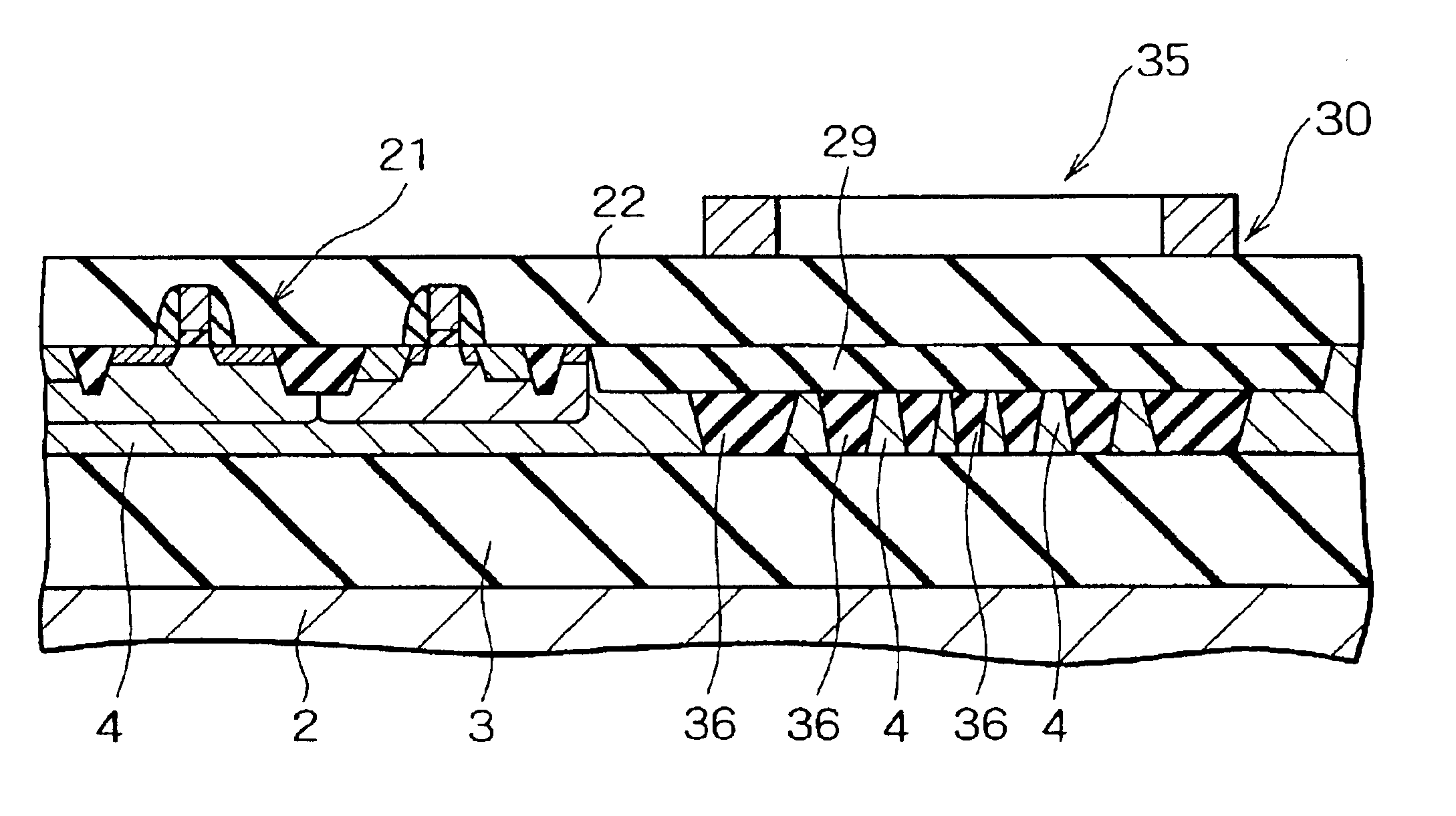
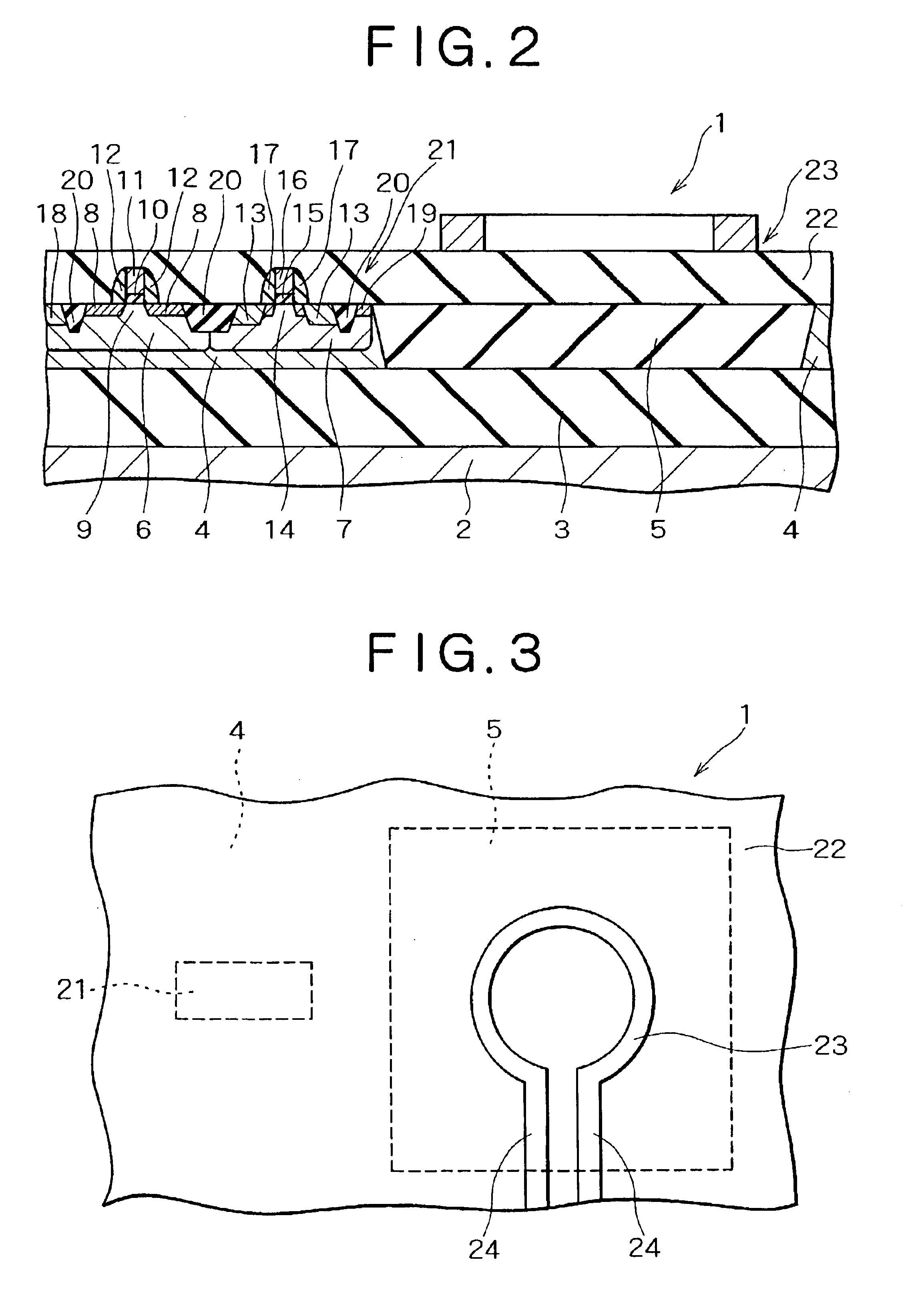
An insulating film 22 is provided above the insulating film 26 and over the CMOS 21, so as to cover the CMOS 21. The bottom surface of the insulating film 22 makes contact with the top surface of the insulating film 26. In addition, an inductor 23 is formed in a region on the insulating film 22, located away from a region above the CMOS 21, that is to say, in a region corresponding to the insulating film 26. The configurations of the insulating film 22 and the inductor 23 are the same as the configurations of insulating film 22 and inductor 23 according to the above-described

As shown in FIG. 6, the inductor 23 is a wire having one winding in a circular loop-form, of which the inner diameter is, for example, 50 μm and the wire width is, for example, 10 μm. Terminal portions 24, making up a pair, are connected to the respective ends of the inductor 23. In addition, as shown in FIG. 6, the insulating film 22 is provided under the inductor 23 and the terminal portions 24, and the insula...

third embodiment

An insulating film 22 is provided above the insulating film 29 and over the CMOS 21, so as to cover the CMOS 21. The bottom surface of the insulating film 22 makes contact with the top surface of the insulating film 29. In addition, an inductor 30 is formed in a region on the insulating film 22 located away from the CMOS 21, that is to say, in a region corresponding to the insulating film 29. The configurations of the insulating films 22 and the inductor 30 are the same as the configurations of the insulating films 22 and the inductor 30 according to the above-described

As shown in FIG. 12, the inductor 30 is a wire in a square loop form having one winding and is made of aluminum, wherein the longitudinal and transverse lengths of the inner dimensions of the wire loop are, for example, 50 μm, the width of the wire is, for example, 10 μm and the thickness of the wire is, for example, 2 μm. Terminal portions 24, making up a pair, are, respectively, connected to the ends of the inductor...


PUM


Abstract

A semiconductor substrate made of P type or P−− type silicon having a thickness of approximately 700 μm and a resistivity of 10 Ω·cm to 1000 Ω·cm is provided, a BOX layer with a thickness of 0.2 μm to 10 μm is provided on the semiconductor substrate and a p type SOI layer is provided on this BOX layer. A first insulating film, which makes contact with the BOX layer, is locally buried in this p type SOI layer and a CMOS is formed in a region of the p type SOI layer wherein the above-described first insulating film is not provided. A second insulating film is provided above the first insulating film and over the CMOS, so as to cover the CMOS, and an inductor is provided on the region of this second insulating film corresponding to the first insulating film.

Description

BACKGROUND OF THE INVENTION1. Field of the InventionThe present invention relates to an integrated circuit provided with an active element, such as a CMOS (complementary metal oxide semiconductor), a TFT (thin film transistor), or the like, and provided with an inductor as well as to a manufacturing method for the same, in particular, relates to an integrated circuit wherein an increase in speed of an active element is achieved and wherein an improvement in the characteristics of an inductor is achieved as well as to a manufacturing method thereof.2. Description of the Related ArtAn integrated circuit provided with an active element, such as a CMOS, a TFT, or the like, wherein an inductor has conventionally been fabricated on a standard substrate and an epitaxial layer including P type impurities is formed on a P+ bulk substrate.FIG. 1 is a cross sectional view showing a conventional integrated circuit. A standard substrate wherein a P− epitaxial layer 52 is formed on a P+ bulk subs...

Claims


Application Information

Patent Timeline
IPC IPC(8): H01L27/12H01L21/70H01L21/84H01L27/06H01L21/76H01L21/822H01L21/8234H01L21/762H01L21/8238H01L27/04H01L27/08H01L27/092H01L29/786
CPCH01L21/84H01L27/1203H01L27/0617H01L27/04
Inventor OHKUBO, HIROAKINAKASHIBA, YASUTAKA
Owner RENESAS ELECTRONICS CORP
Why Eureka
Try Eureka