Recording medium, recording apparatus and recording method

a recording apparatus and recording medium technology, applied in mechanical recording, nanoinformatics, instruments, etc., can solve the problems of inability to realize a recording density on inability to realize a recording density of the order of terabits/cm, etc., to achieve a higher recording density and increase the effect of conductivity

Inactive Publication Date: 2005-02-01
KK TOSHIBA
View PDF23 Cites 41 Cited by
  • Summary
  • Abstract
  • Description
  • Claims
  • Application Information

AI Technical Summary

Benefits of technology

An object of the present invention is to provide a recording medium, a recording apparatus and a recording method capable of achieving a super high recording density.
In the present invention, the first material capable of accumulating the charge includes electron donative or acceptive organic materials, metals, alloys, semiconductors and dielectrics. Also, the second material used in the present invention, which is not particularly limited as far as the conductivity is increased by light absorption, is generally provided by a material that is an insulator when the material is not irradiated with light and is converted into a conductive material upon irradiation with light. In the case of using a material whose conductivity is non-linearly changed in accordance with the intensity of the light as the second material, it is possible to achieve a higher recording density.

Problems solved by technology

In such a technology, however, a drastically high recording density has not yet been realized.
In addition, the energy required for the recording is large.
Therefore, it is considered impossible to realize a recording density on the order of terabits / cm2, which requires recording marks of about 10 nm.
However, it is difficult to achieve a recording density on the order of terabits / cm2, which requires a recording mark of about 10 nm, in this method, too.
In other words, the recording tends to be broken.
Further, since the recording layer has a uniform composition in the recording medium, the difference in signal intensity is small between the crystal region and the amorphous region, giving rise to a large noise.
The problem of noise generation takes place not only in the heat mode recording medium but also in the photon mode recording medium having a uniform composition in the recording layer.
However, in this recording medium, it is difficult to form dot-like recording regions of a uniform size and to arrange regularly the dot-like recording regions.
However, it is generally difficult to achieve the required smoothness.
Also, even if the required surface smoothness is achieved by forming a protective layer on that surface of the recording medium on which the dot-like recording regions are formed, a new problem is brought about that a high voltage is required for injecting and discharging electric charges into and from the recording regions.
As described above, various problems remain unsolved in the conventional recording technology that it is impossible to form a small recording mark, that a large energy is required for the recording of information and for the reproduction of recorded information, that the recorded information tends to be broken, that a large noise is generated, and that it is difficult to make the surface of the recording layer smooth.
Under the circumstances, a recording technology capable of achieving a super high recording density has not yet been put to a practical use.

Method used


Image

  • Recording medium, recording apparatus and recording method
  • Recording medium, recording apparatus and recording method
  • Recording medium, recording apparatus and recording method

Examples


second embodiment

the present invention will now be described.

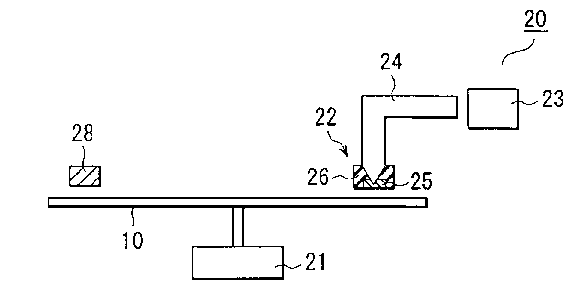
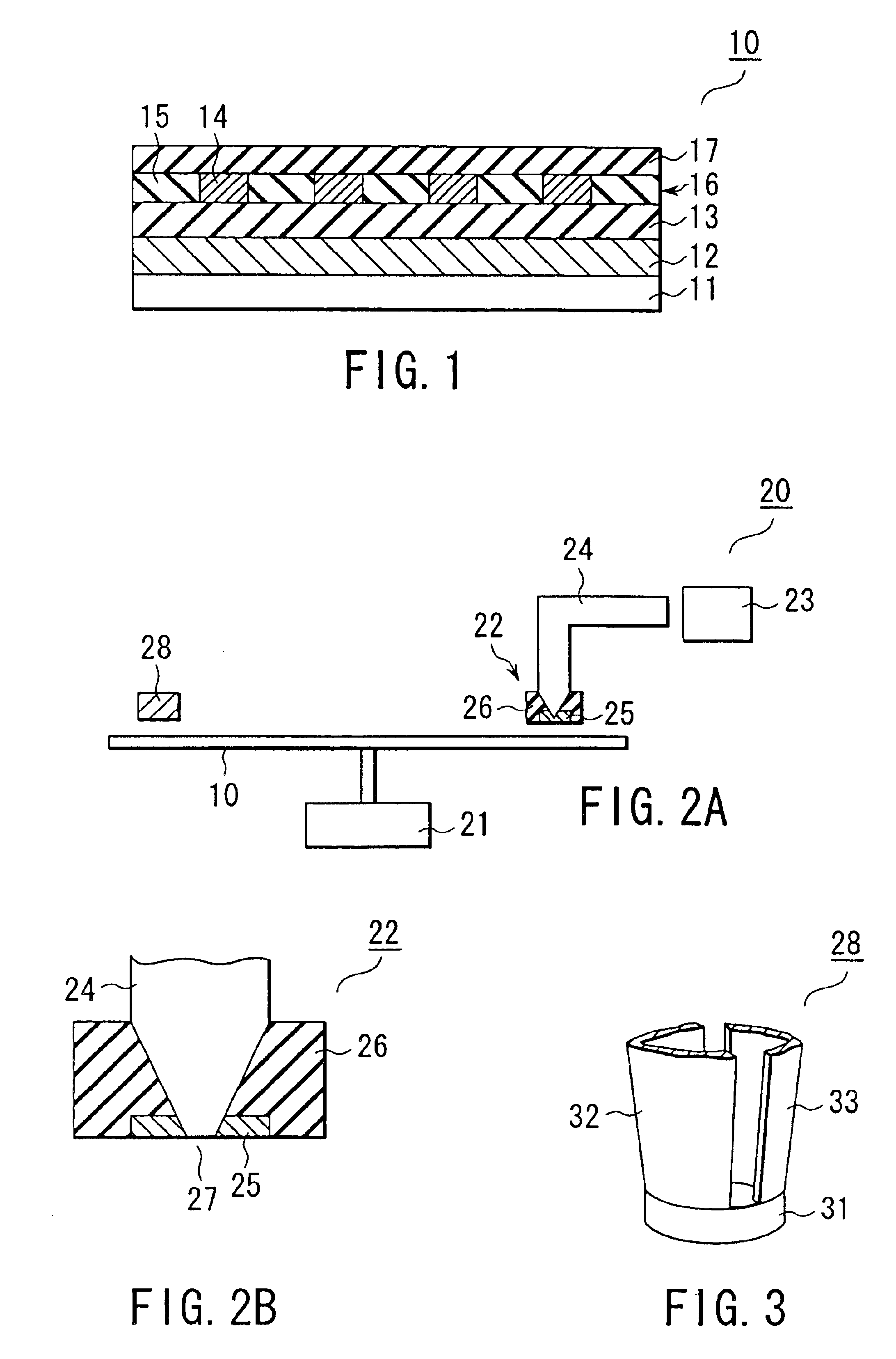
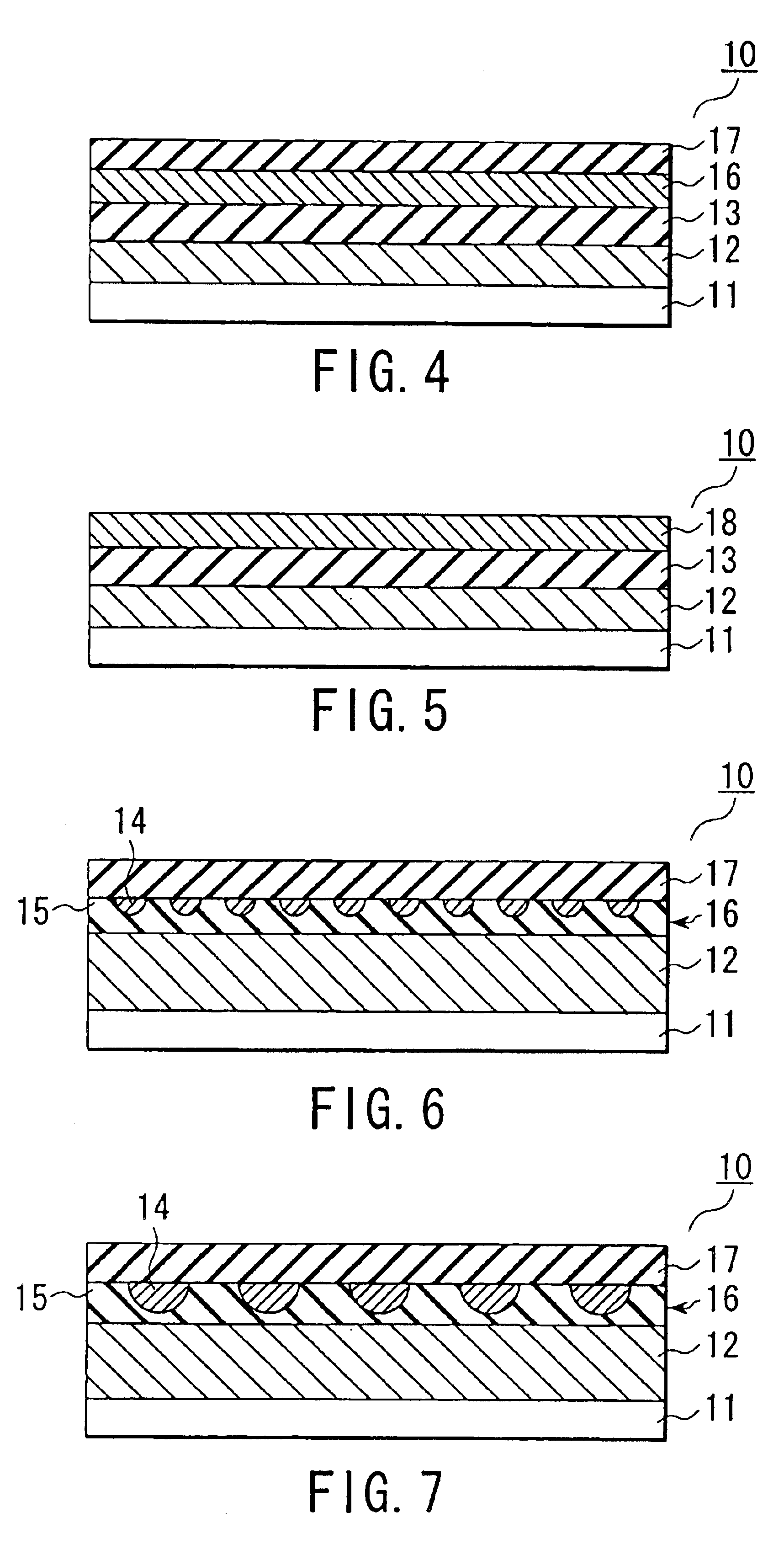
FIG. 4 is a cross sectional view schematically showing a recording medium 10 according to a second embodiment of the present invention. The recording medium 10 shown in FIG. 4 has a structure that a conductive layer 12, an insulating layer 13, a recording layer 16, and a photoconductive layer 17 are stacked on a substrate 11 in the order mentioned. In the recording medium 10 of the particular construction, the recording layer 16 is constructed such that a large number of fine charge accumulating regions (not shown) are uniformly dispersed in an electrically insulating region (not shown). Naturally, the adjacent charge accumulating regions are electrically insulated from each other by the electrically insulating region. In other words, the second embodiment differs from the first embodiment in the construction of the recording layer 16. Also, a plurality of charge accumulating regions correspond to one bit in the second embodiment.

The recor...

third embodiment

the present will now be described.

Specifically, FIG. 5 is a cross sectional view schematically showing the construction of a recording medium 10 according to the third embodiment of the present invention. As shown in the drawing, the recording medium 10 in this embodiment has a structure that a conductive layer 12, an insulating layer 13, and a photoconductive recording layer 18 are stacked on a substrate 11 in the order mentioned. The third embodiment differs from the first and second embodiments in that the photoconductive recording layer 18 is used in the third embodiment in place of the laminate structure of the recording layer 16 and the photoconductive layer 17. In the photoconductive recording layer 18, photoconductive regions (not shown) and charge accumulating regions (not shown) are dispersed in an electrically insulating region (not shown). Also, in the third embodiment, a plurality of charge accumulating regions correspond to one bit.

The recording medium 10 shown in FIG....

fourth embodiment

the present invention will now be described.

Specifically, FIG. 6 is a cross sectional view schematically showing the construction of a recording medium 10 according to the fourth embodiment of the present invention. The recording medium 10 shown in FIG. 6 has a structure that a conductive layer 12, a recording layer 16, and a photoconductive layer 17 are stacked on a substrate 11 in the order mentioned. The fourth embodiment differs from the first embodiment in that the insulating layer 13 is not formed in the fourth embodiment. Also, the recording layer 16 is constituted by an electrically insulating region (insulating layer) 15 having a plurality of pits formed on the surface and a plurality of electrically insulating regions 14 filling these pits. Also, in this embodiment, each of the plural charge accumulating regions 14 corresponds to one bit.

The recording medium 10 shown in FIG. 6 can be manufactured, for example, as follows.

In the first step, a glass disc having an optical fi...


PUM

PropertyMeasurementUnit
diameteraaaaaaaaaa
diameteraaaaaaaaaa
thicknessaaaaaaaaaa

Abstract

The present invention provides a recording medium having a plurality of charge accumulating regions each containing a first material capable of accumulating an electric charge and a photoconductive region containing a second material whose conductivity is increased by light absorption, a recording apparatus including such a recording medium, and a method recording information on such a recording medium. In the present invention, information is recorded on the recording medium by irradiating the photoconductive region with light and by injecting an electric charge into the charge accumulating region via that portion of the photoconductive region which is irradiated with light.

Description

CROSS-REFERENCE TO RELATED APPLICATIONSThis application is based upon and claims the benefit of priority from the prior Japanese Patent Application No. 11-277456, filed Sep. 29, 1999, the entire contents of which are incorporated herein by reference.BACKGROUND OF THE INVENTIONThe present invention relates to a recording medium, a recording apparatus and a recording method.In the information society in recent years, the amount of information is on a sharp increase. Therefore, it is of very high importance to develop a recording method or a recording apparatus capable of drastically improving the recording density, compared with the prior art.As a technology for realizing a high recording density, attentions are paid to an optical recording such as a heat mode recording in which light is converted into heat for performing the recording or a photon mode recording in which recording is performed without converting light into heat.As a heat mode recording, a magneto-optic recording or a ...

Claims


Application Information

Patent Timeline
Patent Type & Authority Patents(United States)
IPC IPC(8): G11B9/08G11B9/00G11B13/00G11B13/06B82B1/00G11B7/24035G11B9/14G11B11/08
CPCB82Y10/00G11B9/08G11B13/06G11B9/1409
Inventor NAITO, KATSUYUKIHIEDA, HIROYUKI
Owner KK TOSHIBA
Why Eureka
Try Eureka