Fabrication method for semiconductor hole

a technology of semiconductor holes and fabrication methods, which is applied in the direction of photomechanical treatment, instruments, electrical equipment, etc., can solve the problems of affecting the actual amount of exposure light to the photoresist, affecting the pattern density, and generating defects in the dielectric layer in the subsequent process, so as to prevent the peeling of the photoresist

Inactive Publication Date: 2005-02-08
MACRONIX INT CO LTD
View PDF4 Cites 26 Cited by
  • Summary
  • Abstract
  • Description
  • Claims
  • Application Information

AI Technical Summary

Benefits of technology

Accordingly, the present invention provides a method for fabricating a hole in a semiconductor device, wherein aerial ima...

Problems solved by technology

On the other hand, proximity effect is a result from the interference between light beams due to the reflection of light from the substrate of a wafer through the photoresist on the wafer surface.
The reflected light, however, would lead to multiple exposures to the photoresist, alt...

Method used


Image

  • Fabrication method for semiconductor hole
  • Fabrication method for semiconductor hole
  • Fabrication method for semiconductor hole

Examples


Embodiment Construction

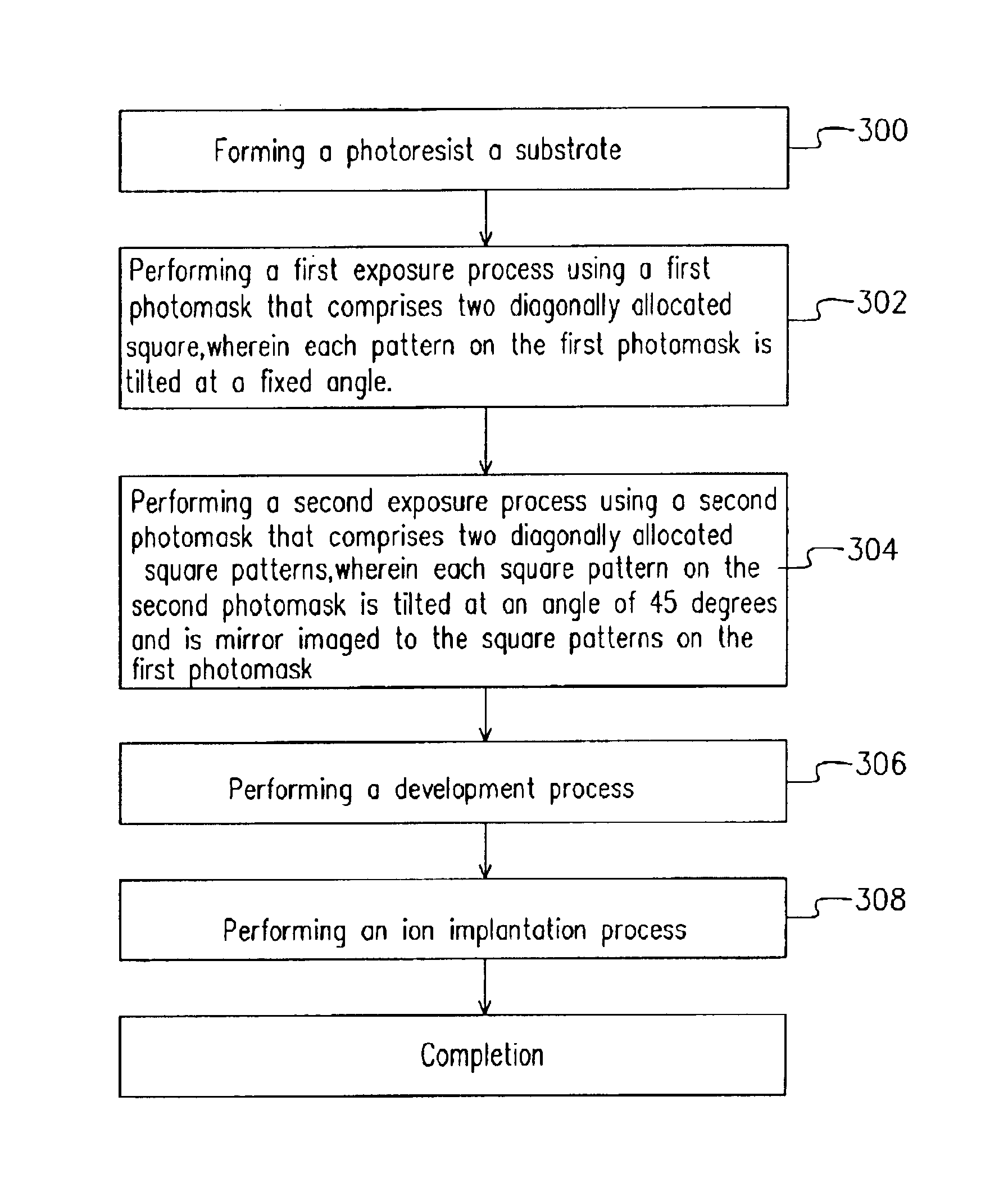
FIG. 3 a flow diagram illustrating the process flow for fabricating a semiconductor hole according to one embodiment of the present invention.

Referring to FIG. 3, in step 300, a photoresist is formed on a substrate, wherein the substrate comprises, for example, a semiconductor substrate, a semiconductor device, a conductive layer, a dielectric layer, etc. In one example, step 300 can include forming a semiconductor device on a semiconductor substrate, followed by forming a dielectric layer on the semiconductor substrate to cover the semiconductor device. The dielectric layer is then planarized, followed by forming a photoresist layer on the planarized dielectric layer.

Thereafter, in step 302, a first exposure is performed using a first photomask that comprises two diagonally allocated polygon patterns, wherein each polygon pattern on the first photomask is rotated a fixed angle from its arrayed position. The photomask of the present invention comprises square patterns, which are exp...


PUM


Abstract

A fabrication method for a semiconductor hole is described. The method provides a circular or a elliptical hole pattern. A first exposure is performed with a first photomask that comprises a plurality of diagonally allocated square patterns wherein the square patterns on the first photomask are tilted at an angle of 45 degrees. Thereafter, a second exposure is performed using a second photomask, wherein patterns on the second photomask are mirror images to those on the second photomask to prevent the peeling of the photoresist at between the diagonally allocated hole patterns.

Description

CROSS REFERENCE TO RELATED APPLICATIONSThis application claims the priority benefit of Taiwan application serial no. 91112176, filed Jun. 6, 2002.BACKGROUND OF INVENTION1. Field of the InventionThe present invention relates to the patterning of a semiconductor device. More particularly, the present invention relates to a method for forming a semiconductor hole.2. Background of the InventionA prevailing tendency in the semiconductor industry is to reduce the design dimension of the circuitry devices. Photolithography thereby becomes a significant step in the entire semiconductor manufacturing. Anything that is related to the structure of a semiconductor device, for example, the patterning of each layer of thin film, the critical dimension is determined by the photolithography process. In other words, the critical dimension of a device is determined by the advancement of the photolithography technique. Thus, the accuracy in the transferring of a photomask pattern plays an important ro...

Claims


Application Information

Patent Timeline
IPC IPC(8): H01L21/02H01L21/4763H01L21/027
CPCH01L21/0274
Inventor WU, TSUNG-HSIEN
Owner MACRONIX INT CO LTD
Why Eureka
Try Eureka