Semiconductor device fabrication method and semiconductor device fabrication apparatus

a semiconductor device and fabrication method technology, applied in the direction of individual semiconductor device testing, semiconductor/solid-state device testing/measurement, instruments, etc., can solve the problems of product damage, the remaining portion of the matrix substrate cannot be divided into a remaining portion and the dividing portion, so as to improve product quality, reduce the cost of semiconductor devices, and reduce the working cost

Inactive Publication Date: 2005-02-08
RENESAS ELECTRONICS CORP +1
View PDF12 Cites 13 Cited by
  • Summary
  • Abstract
  • Description
  • Claims
  • Application Information

AI Technical Summary

Benefits of technology

Thus, after substrate division, a pulling force can be exerted on the wiring patterns by a series of associated operations, with the result that both substrate division and tearing-off of the wiring pattern can be done stably and automatically without causing any damage to products.
Consequently, it becomes possible to automate the matrix substrate dividing work and hence possible to reduce the working cost.

Problems solved by technology

According to the above substrate dividing methods, however, in a matrix substrate having dividing grooves, if wiring patterns which span such dividing grooves are formed on the back side of the matrix substrate, the wiring patterns will not be cut completely even if a dividing portion in the matrix substrate is bent for division along the associated dividing groove, thus giving rise to the problem that the ma

Method used


Image

  • Semiconductor device fabrication method and semiconductor device fabrication apparatus
  • Semiconductor device fabrication method and semiconductor device fabrication apparatus
  • Semiconductor device fabrication method and semiconductor device fabrication apparatus

Examples


second embodiment

As to detailed contents of operations performed respectively in the assembling steps, reference will be made thereto later in the present invention.

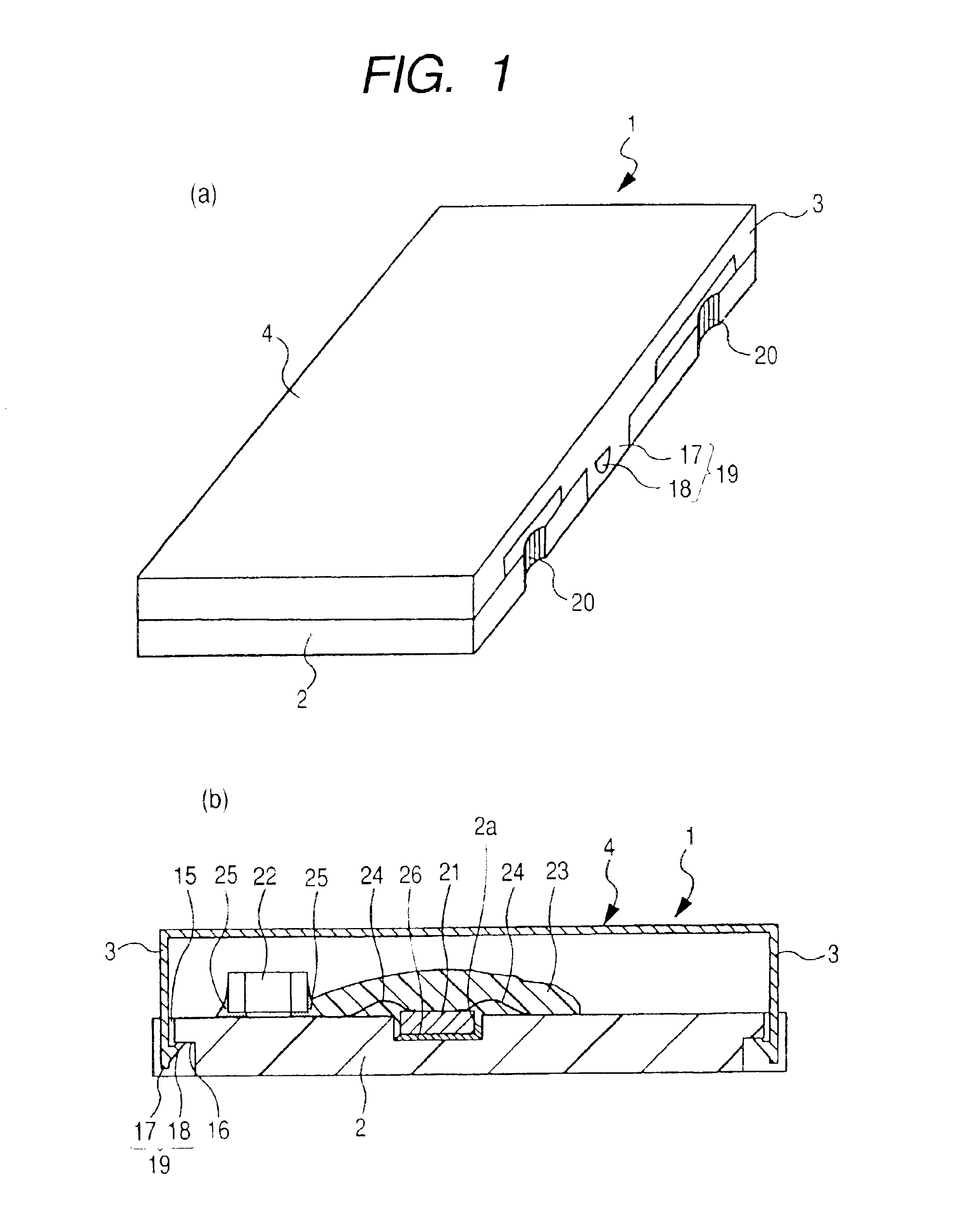
In this first embodiment, the high-frequency module 1 is assembled by the following method which is characteristic throughout the whole of the high-frequency module manufacturing process.

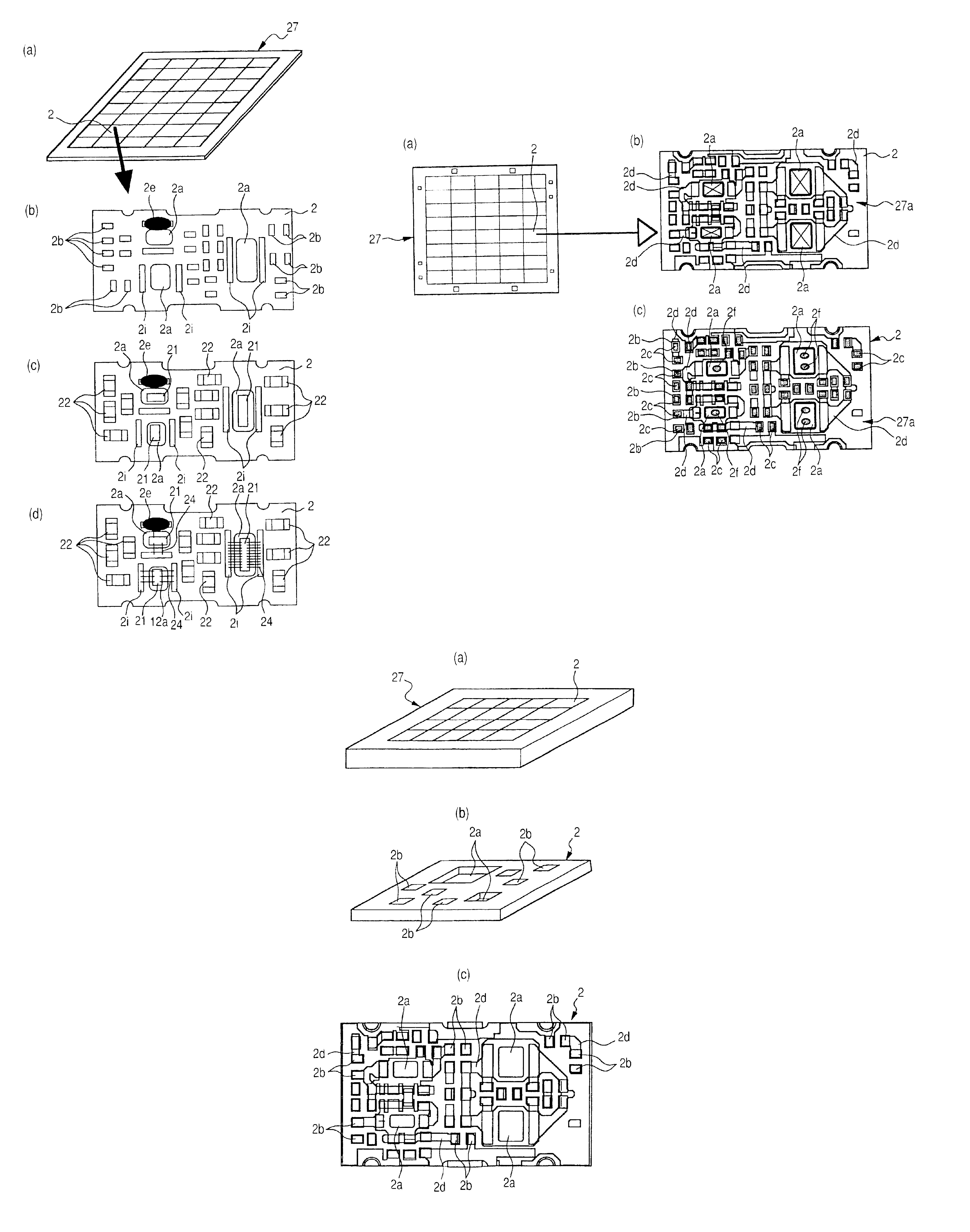
First, chip parts 22 and semiconductor pellets 21 are disposed on each of only inspection-passed wiring substrates on the matrix substrate 27 shown in FIG. 5(a). Thus, the chip parts 22 and the semiconductor pellets 21 are disposed on only non-defective wiring substrates 2. That is, in the cap inserting step S10, the cap 4 is attached to only each non-defective wiring substrate 2.

More specifically, such a defect mark 2e as shown in FIG. 5(a) is affixed to a block, i.e., wiring substrate 2, which is judged to be defective in a delivery (purchasing) stage inspection of wiring substrates 2 on the matrix substrate 27 (it is optional whether this inspection i...


PUM


Abstract

A method of manufacturing a semiconductor device able to reduce the number of manufacturing steps and attain the rationalization of a manufacturing line is disclosed. The semiconductor device is a high-frequency module assembled by mounting chip parts (22) and semiconductor pellets (21) onto each of wiring substrates (2) formed on a matrix substrate (27) after inspection. A defect mark (2e) is affixed to a wiring substrate (2) as a block judged to be defective in the inspection of the matrix substrate (27), then in a series of subsequent assembling steps the defect mark (e) is recognized and the assembling work for the wiring substrate (2) with the defect mark (2e) thereon is omitted to attain the rationalization of a manufacturing line.

Description

TECHNICAL FIELDThe present invention relates to a semiconductor manufacturing technique and more particularly to a technique which is effectively applicable to a high-frequency module (a high-frequency power amplifier) manufacturing method and a semiconductor manufacturing apparatus used therein.BACKGROUND ARTAs to a high-frequency power amplifier called a high-frequency module (also called RF module or RF power module) on which are mounted surface-mounted type chip parts such as chip capacitor and chip resistor and also mounted bare chip-mounting semiconductor pellets, it is described, for example, in Japanese Unexamined Patent Publication No. Hei 10(1998)-12808 (Numanami). In this publication there are described a structure and electrical characteristics of a high-frequency module and a structure of a matrix substrate for assembling plural high-frequency modules at a time.As to a cap mounting method in a hybrid IC (integrated circuit), a description thereof is found, for example, ...

Claims


Application Information

Patent Timeline
IPC IPC(8): H01L21/02H01L23/50H01L21/50H01L21/66H01L23/02H01L23/13H01L23/544H01L23/10H01L23/48H01L23/12H01L23/498G01R31/26H01L21/58H01L21/98H01L23/04H01L25/16
CPCH01L21/50H01L23/04H01L23/10H01L23/13H01L23/49805H01L23/50H01L23/544H01L24/97H01L25/16H01L25/165H01L25/50H01L22/20H01L2924/1306H01L2223/54406H01L2223/54473H01L2223/54486H01L2224/48091H01L2224/73265H01L2224/97H01L2924/01013H01L2924/01015H01L2924/01029H01L2924/0103H01L2924/01033H01L2924/01047H01L2924/01074H01L2924/01078H01L2924/01079H01L2924/01082H01L2924/014H01L2924/10329H01L2924/14H01L2924/15153H01L2924/15165H01L2924/15313H01L2924/15787H01L2924/16152H01L2924/16315H01L2924/19041H01L2924/19043H01L2924/19105H01L2224/45144H01L24/48H01L2924/01005H01L2924/01006H01L2924/01023H01L2224/32225H01L2224/48227H01L2224/85H01L2924/00014H01L2224/83H01L2924/00H01L2924/00012H01L2924/12042H01L24/45H01L24/73H01L2924/181H01L2224/83192H01L2224/92247H01L2224/49175H01L2224/05599H01L2224/32245H01L2224/48247
Inventor ISHIZU, AKIOTAKASHIMA, KAZUTOSHIOBA, SHIROKOBAYASHI, YOSHIHIKOIDA, TSUTOMUHAGA, SHIGERUTAKADA, SUSUMUKOUJIRO, IWAMICHIARAI, NORINAGAKAKEGAWA, YUJI
Owner RENESAS ELECTRONICS CORP
Why Eureka
Try Eureka