Phase comparator and clock recovery circuit

Inactive Publication Date: 2005-02-08
SOCIONEXT INC
View PDF12 Cites 13 Cited by
  • Summary
  • Abstract
  • Description
  • Claims
  • Application Information

AI Technical Summary

Benefits of technology

Meanwhile, more specifically, the present invention provides a clock recovery circuit generating a clock signal from a supplied data signal, comprising: a frequency divided signal-generating means for generating a frequency divided signal from the data signal; and a phase comparator that receives as input the frequency divided signal, and intermittently performs a phase comparison between the data signal and the clock signal according to the logic level of the frequency divided signal. According to the present invention, the frequency divided signal-generating means generates the frequency divided signal from the data signal, and the phase comparator intermittently performs the phase comparison between the data signal and the clock signal according to the logic level of the frequency divided signal. This makes it possible to increase the timing margin for the phase comparison and to perform the phase comparison for data signals with high-speed bit rates. Accordingly, it becomes possible to achieve a clock recovery circuit that supports high-speed bit rates.
Preferably, in the above-described clock recovery circuit, the phase comparator receives as input a speed signal indicating the bit rate of the data signal, and selects whether the phase comparison is to be sequentially performed or to be intermittently performed according to the bit rate indicated by the speed signal. With this configuration, the phase comparator can select whether the phase comparison between the first signal and the second signal is to be sequentially performed or to be intermittently performed according to the bit rate of the data signal that is indicated by the speed signal. This configuration achieves a clock recovery circuit that can support a wide range of data signals with low-speed bit rates as well as high-speed bit rates. In addition, since the clock recovery circuit supports a wide range of bit rates, the degree of circuit designing increases.
Preferably, the clock recovery circuit may further comprises a charge pump circuit that receives as input a phase difference signal indicating the result of the phase comparison, and outputs a current having an amount that is determined based on the phase difference signal. The charge pump circuit receives as input a speed signal indicating the bit rate of the data signal, and changes the amount of the current according to the bit rate indicated by the speed signal. With this configuration, the amount of the current that is output from the charge pump circuit is changed according to the bit rate of the data signal indicated by the speed signal. Thus, the loop gain of the PLL in the clock recovery circuit can be kept constant.
Furthermore, it is preferable that the clock recovery circuit comprises a speed signal-generating means that compares the frequency of a supplied reference signal and the frequency of an internal signal of the clock recovery circuit, and generates the speed signal based on the result of the comparison. With this configuration, the frequency of the supplied reference signal and the frequency of the internal signal of the clock recovery circuit are compared by the speed signal-generating means, and the speed signal is generated based on the result of the comparison. As a result of this, in the clock recovery circuit, the terminal to which the speed signal is input from outside can be eliminated, the number of pads can be reduced, and circuit designing is facilitated.
Meanwhile, specifically, the present invention also provides a clock recovery circuit generating a clock signal from a supplied data signal, comprising: a frequency divided signal-generating

Problems solved by technology

However, when the bit rate is at high speed and in the order of one gigabit per second, the above-described phase comparison can cause problems.
If such cases arise, signal racing ta

Method used


Image

  • Phase comparator and clock recovery circuit
  • Phase comparator and clock recovery circuit
  • Phase comparator and clock recovery circuit

Examples


Example

Embodiment 1

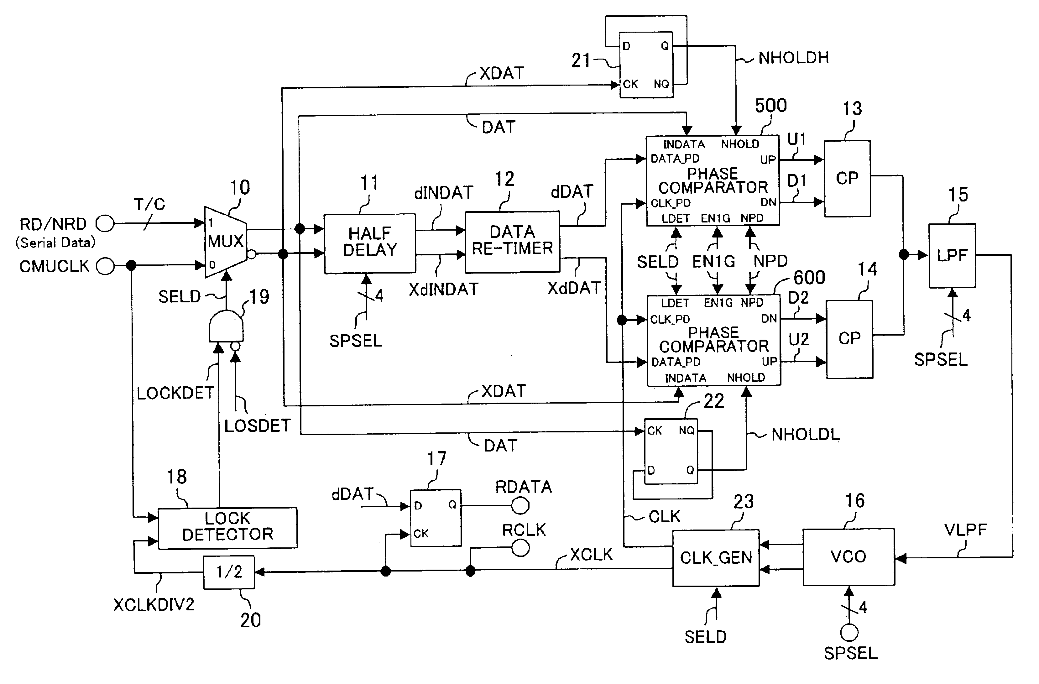
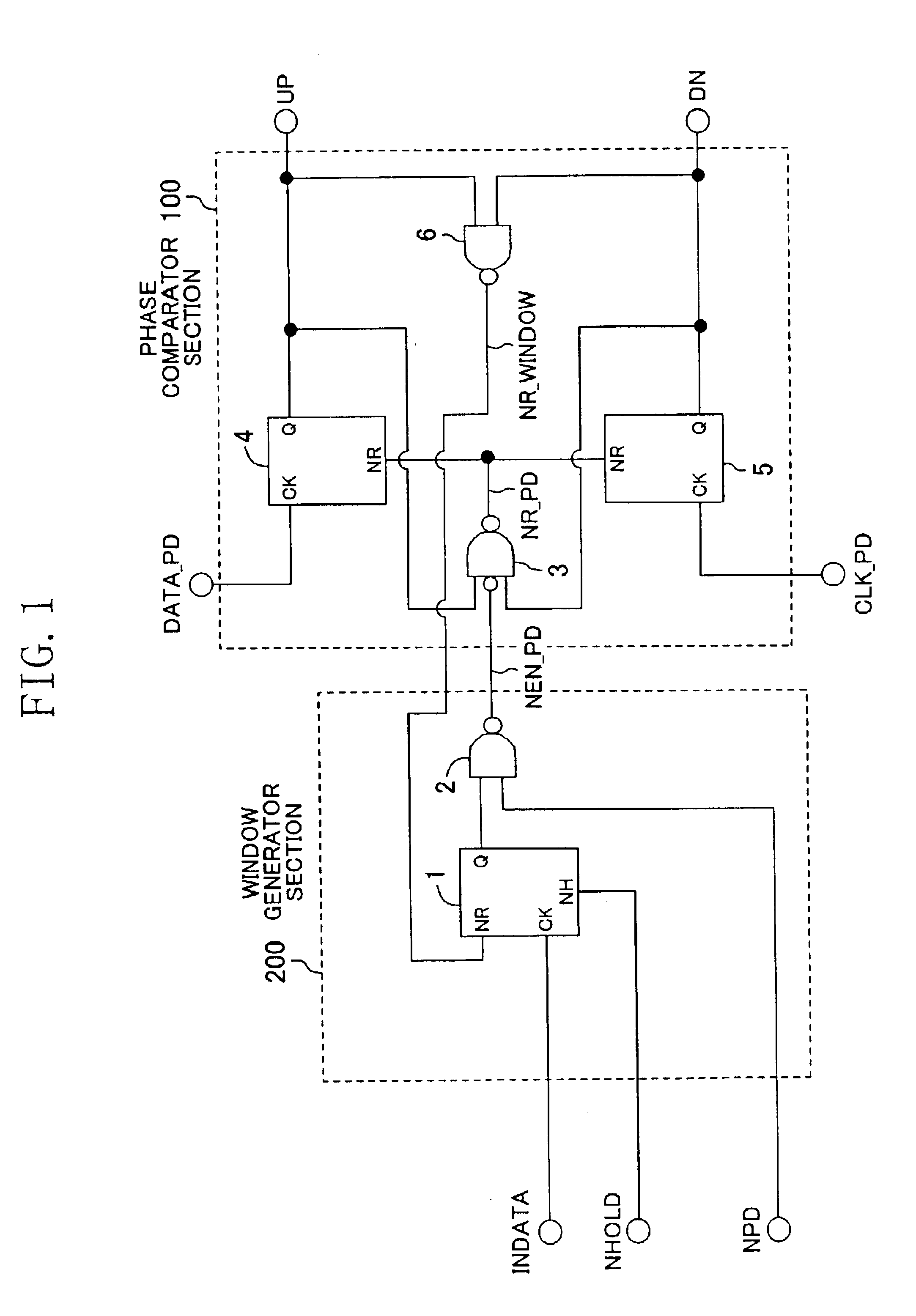
FIG. 1 shows a circuit diagram of a phase comparator according to Embodiment 1 of the present invention. The phase comparator according to the present embodiment comprises a phase comparator section 100 and a window generator section 200, and it intermittently performs a phase comparison between the rising edge of a data signal DATA_PD, which is a comparison subject, and the rising edge of a clock signal CLK_PD, which is another comparison subject. The result of the phase comparison is represented as the difference between the pulse width of a signal UP and a signal DN. It should be noted that the data signal DATA_PD and the clock signal CLK_PD correspond to the first signal and the second signal of the present invention, respectively.

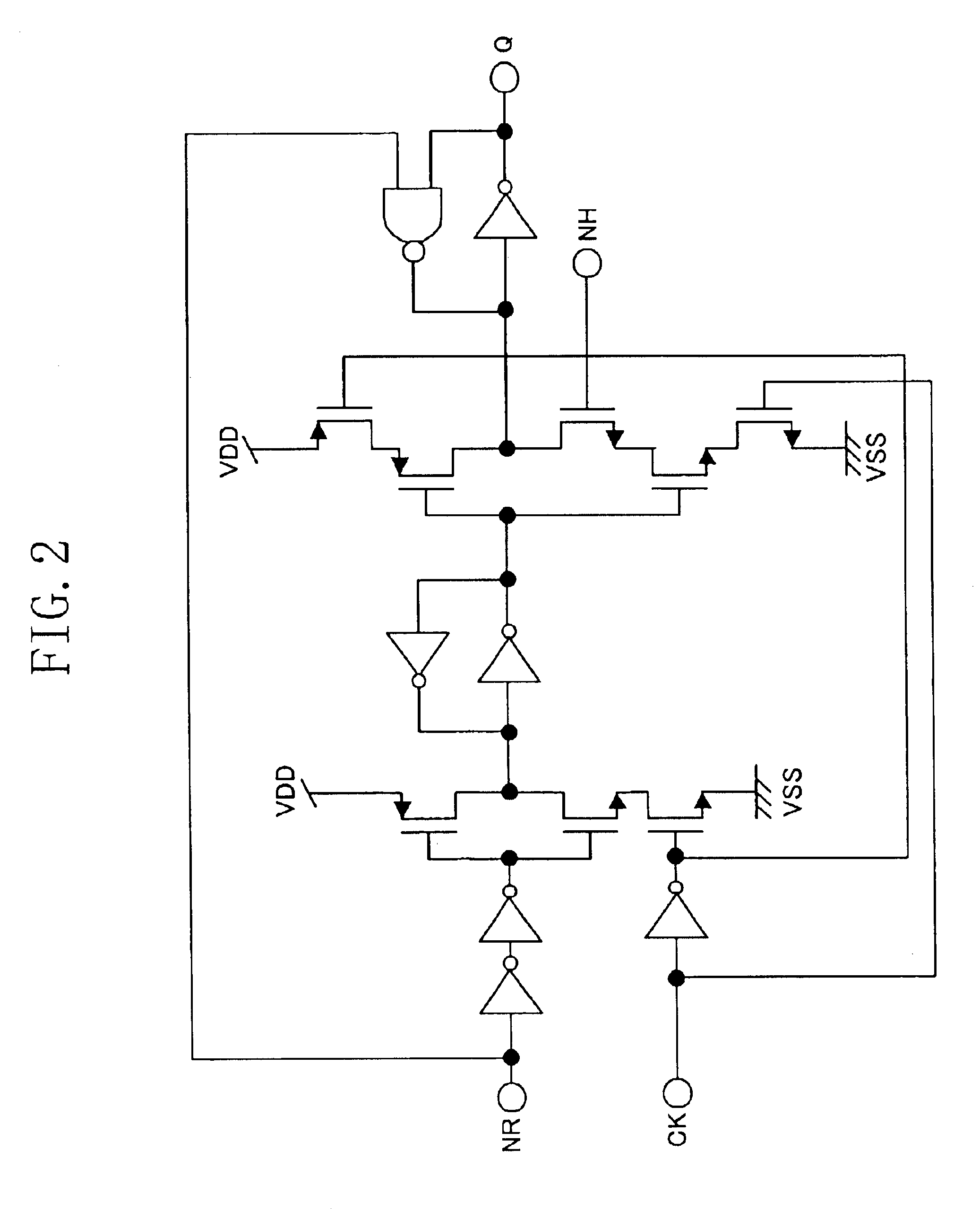
The window generator section 200 is composed of a latch circuit 1 and a NAND circuit 2. In the latch circuit 1, a signal INDATA is input into an input CK; a signal INHOLD, which corresponds to the frequency divided signal of the present inv...

Example

Embodiment 2

FIG. 5 shows the circuit diagram of a phase comparator according to Embodiment 2 of the present invention. The phase comparator according to the present embodiment comprises a window generator section 200A having a selector circuit 7, which corresponds to the activating means of the present invention, between the latch circuit 1 and the NAND circuit 2 of the phase comparator shown in FIG. 1.

The selector circuit 7 receives as input a signal LDET, which corresponds to the frequency comparison signal of the present invention. It selects the input signal to the NAND circuit 2 according to the logic level of the signal LDET. More specifically, when the signal LDET is at “H”, it inputs the output signal from the latch circuit 1 into the NAND circuit 2. By contrast, when it is at “L”, the input to the NAND circuit 2 is fixed at “H”.

When the signal LDET is at “H”, the phase comparator according to the present embodiment is similar to the phase comparator according to Embodiment ...

Example

Embodiment 3

FIG. 6 shows the circuit diagram of a phase comparator according to Embodiment 3 of the present invention. The phase comparator according to the present embodiment comprises a window generator section 200B having a NAND circuit 8, which corresponds to the mask means of the present invention, between the input NH of the latch circuit 1 and the terminal NHOLD in the phase comparator shown in FIG. 5.

The NAND circuit 8 receives as input a signal EN1G, which corresponds to the intermittent comparison signal of the present invention. In addition to this, it receives as input the NOT of the signal NHOLD and the signal LDET, and outputs the NAND of these to the input NH of the latch circuit 1.

Here, the data signal DATA_PD is assumed to be a signal according to IEEE 1394b. According to IEEE 1394b, the data rate can switch among 125 Mbps, 250 Mbps, 500 Mbps, and 1 Gbps. The signal EN1G is set to “H” only when the bit rate is 1 Gbps, but to “L” in the rest of times. Thus, when the ...


PUM


Abstract

The present invention aims at providing a phase comparator and a clock recovery circuit suitable for applications that support data signals with high-speed bit rates in the order of one gigabit per second. Phase comparators receive frequency divided signals NHOLDH and NHOLDL generated from a data signal RD/NRD, respectively, and intermittently perform a phase comparison between a signal dDAT and a signal CLK. This increases the timing margin for the phase comparison and makes it possible to perform a phase comparison for high-speed bit rate signals. The provision of phase comparators that serve as clock recovery circuits makes it possible to handle data signals with high-speed bit rates in the order of one gigabit per second.

Description

BACKGROUND OF THE INVENTIONThe present invention relates to phase comparators and clock recovery circuits, and more particularly, to techniques of phase comparison and clock recovery for data signals with high-speed bit rates using a simple phase comparison system.High-speed serial data transferring such as typified by IEEE (Institute of Electrical and Electronics Engineers) 1394b requires that the receiving side should reproduce a clock signal in accordance with the frequency and phase of a data signal from the sending side. For this operation, a clock recovery circuit is indispensable. One type of the architecture for such a clock recovery circuit is a simple phase comparison system that performs serial processing.The simple phase comparison system is such that a data signal is input into a reference input of a PLL (Phase Locked Loop), and an input voltage to a voltage controlled oscillator (VCO) is controlled to match the phases of the data signal and a clock signal that has been...

Claims


Application Information

Patent Timeline
IPC IPC(8): H03D13/00H04L7/033H03L7/08H03K5/26H03L7/087H03L7/089
CPCH04L7/033H03D13/004
Inventor EBUCHI, TSUYOSHIYOSHIKAWA, TAKEFUMIIWATA, TORU
Owner SOCIONEXT INC
Why Eureka
Try Eureka