Multiple circuit blocks with interblock control and power conservation

Inactive Publication Date: 2005-02-08
RENESAS ELECTRONICS CORP
View PDF7 Cites 5 Cited by
  • Summary
  • Abstract
  • Description
  • Claims
  • Application Information

AI Technical Summary

Benefits of technology

In the light of the foregoing, the present invention has been made in order to solve the above-mentioned problems associated with the prior art, and it is therefore an object of the present invention to provide the semiconduc

Problems solved by technology

However, in such a system of reducing the power consumption on the basis of the stop of a clock signal, there is an inconvenience that since the operation of the circuits is stopped while supplying the power source voltage to the chip, if a leakage current occurs in a MOS FET and the like constituting the circuits, this results in that the power consumption is not sufficiently reduced.
For this reason, if each of the circuit blocks on the side of re

Method used


Image

  • Multiple circuit blocks with interblock control and power conservation
  • Multiple circuit blocks with interblock control and power conservation
  • Multiple circuit blocks with interblock control and power conservation

Examples


fourth embodiment

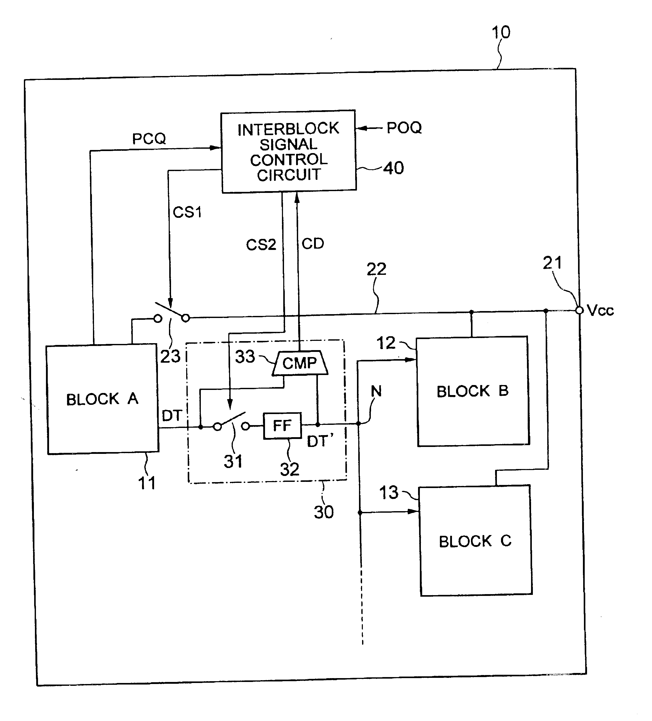
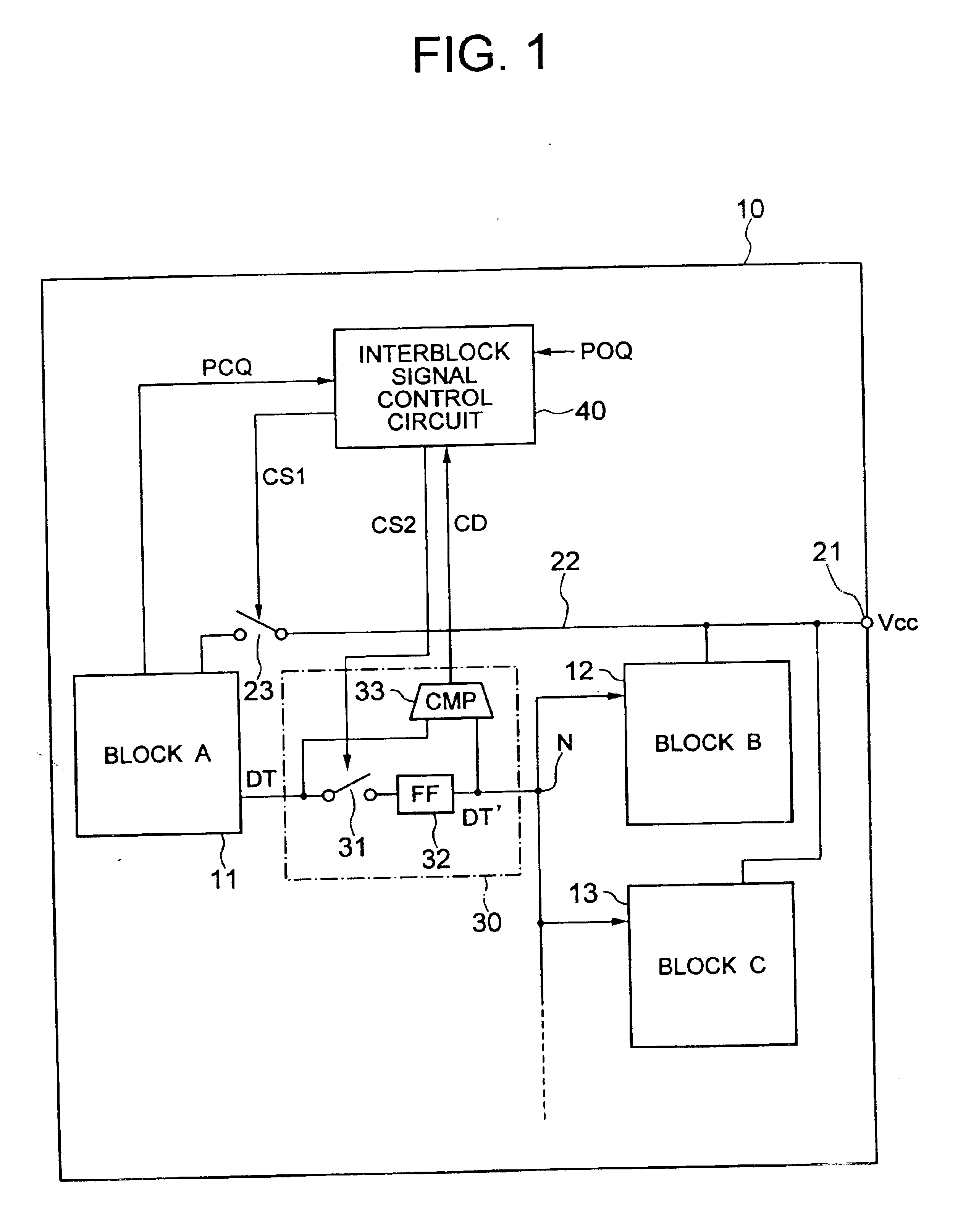
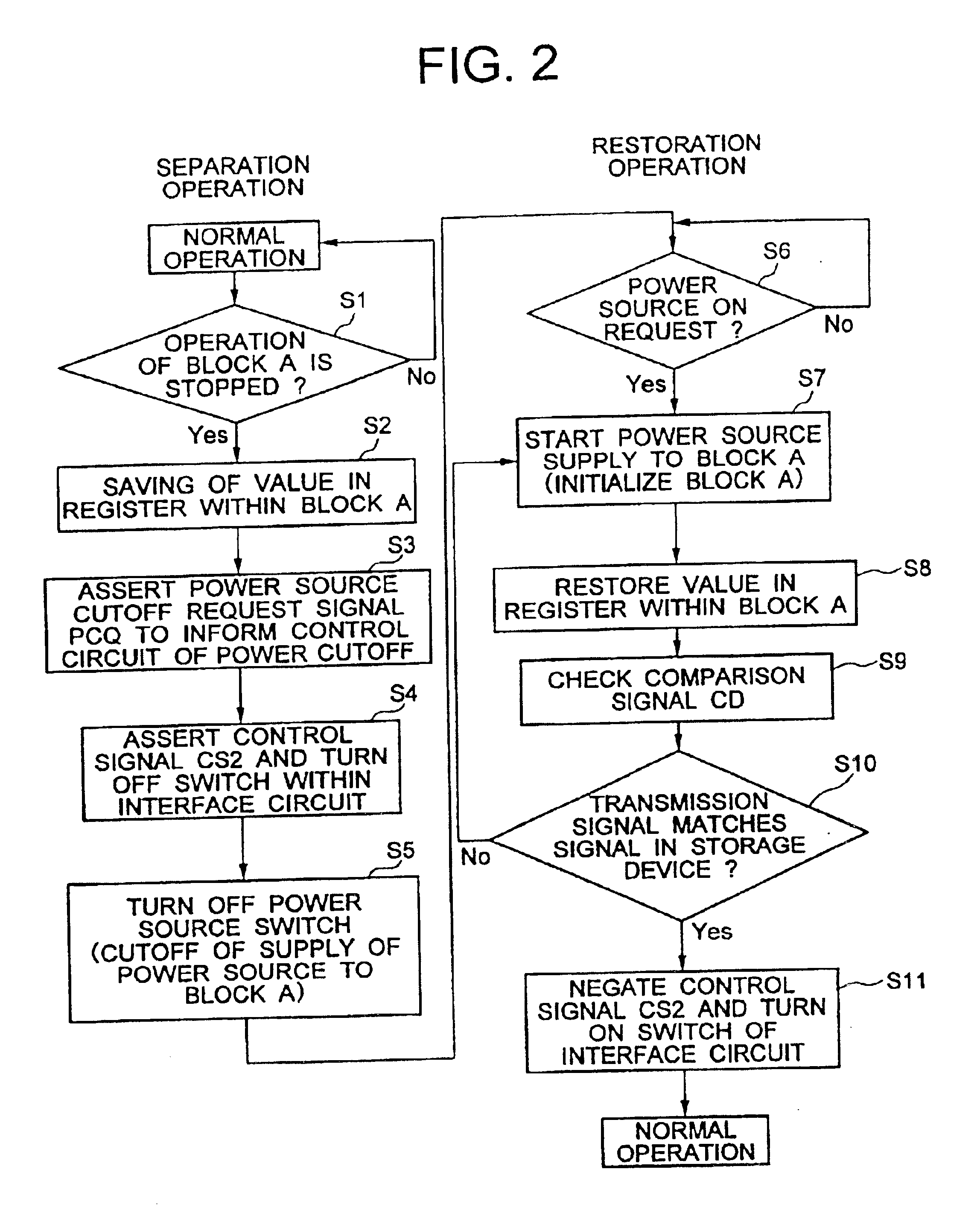
FIG. 8 shows a configuration of a semiconductor IC to which the present invention is applied.

The present embodiment of the semiconductor IC is configured in such a way that when the internal circuit has the circuit block 11 for which the supply of the power source voltage is cut off in accordance with the operation mode and the circuit block 12 which has the power source voltage supplied thereto at all times to be operated, an I / O circuit is divided into an I / O part 131 in which the supply of the power source voltage is cut off in correspondence to the circuit blocks and an I / O part 132 which has the power source voltage supplied thereto at all times to be operated. An interface area 30A in which a plurality of interface circuits 30 as shown in FIG. 1 are arranged is formed between the circuit block 11 and the circuit block 12.

In addition, the present embodiment of the semiconductor IC is also configured in such a way that the signal(s), which does(do) not need to be outputted durin...


PUM


Abstract

A semiconductor integrated circuit is provided including a plurality of circuit blocks and adapted to cut off the supply of power source voltage to any one of the circuit blocks. The integrated circuit includes an interblock interface circuit provided on a signal path from the elected circuit block to other circuit blocks, wherein a single output of the interblock interface circuit is branched out to other circuit blocks. The interblock interface circuit includes a signal gate for preventing signal transmission to other circuit blocks and includes a storage unit for storing a signal right before the power cut.

Description

BACKGROUND OF THE INVENTIONThe present invention relates in general to techniques for reducing power consumption of semiconductor integrated circuits. More particularly, the invention relates to techniques which are effectively utilized in semiconductor integrated circuits for processing data in which, for example, a CPU (Central Processing Unit) and its peripheral circuits are formed on one semiconductor chip, especially, in semiconductor integrated circuits for use in portable or mobile electronic devices which are operated by batteries or cells.Heretofore, there is known a semiconductor IC (Integrated Circuit) such as a microcomputer adapted to stop a clock signal while supplying a power source voltage to the whole chip in a standby mode or the like to stop the operation of the circuits, thereby reducing the power consumption.However, in such a system of reducing the power consumption on the basis of the stop of a clock signal, there is an inconvenience that since the operation o...

Claims


Application Information

Patent Timeline
IPC IPC(8): G06F1/32H01L21/822H01L27/04H03K19/00H03K19/0175
CPCG06F1/32G06F1/3203G06F1/3287Y02B60/1282H01L2924/0002Y02B60/32H01L2924/00Y02D10/00Y02D30/50
Inventor HOSHI, TADASHIHIROSE, KENJIABE, HIDEAKINISHIMOTO, JUNICHINAGAYAMA, MIDORI
Owner RENESAS ELECTRONICS CORP
Why Eureka
Try Eureka