Method of fabricating liquid crystal display

a liquid crystal display and fabrication method technology, applied in the field of liquid crystal display, can solve the problems of increasing the probability of pattern defect generation, increasing the complexity of the process, and increasing the capacitance of the storage capacitor

Inactive Publication Date: 2005-02-08
LG DISPLAY CO LTD
View PDF2 Cites 23 Cited by
  • Summary
  • Abstract
  • Description
  • Claims
  • Application Information

AI Technical Summary

Benefits of technology

In another aspect, forming the perforation hole and the contact hole includes depositing a photoresist on the substrate where the protective film is formed; eliminating the photoresist formed on the drain electrode and forming a photoresist pattern with a first area on the gate line and a photoresist pattern with a second area elsewhere by photolithography using the partial exposure mask at the same time; and eliminating an area of the protective film corresponding to the drain electrode and an area of the protective film corresponding to the first area by use of the photoresist pattern as a mask.

Problems solved by technology

In this case, the process becomes more complicated since a separate storage electrode 24 needs to be formed for the storage capacitor, increasing the probability that a pattern defect may be generated.
Therefore, there is a problem in that the capacitance of the storage capacitor is reduced more because capacitance is proportional to dielectric constant and inversely proportional to the distance between electrodes.

Method used


Image

  • Method of fabricating liquid crystal display
  • Method of fabricating liquid crystal display
  • Method of fabricating liquid crystal display

Examples


Embodiment Construction

Reference will now be made in detail to the preferred embodiments of the present invention, examples of which are illustrated in the accompanying drawings.

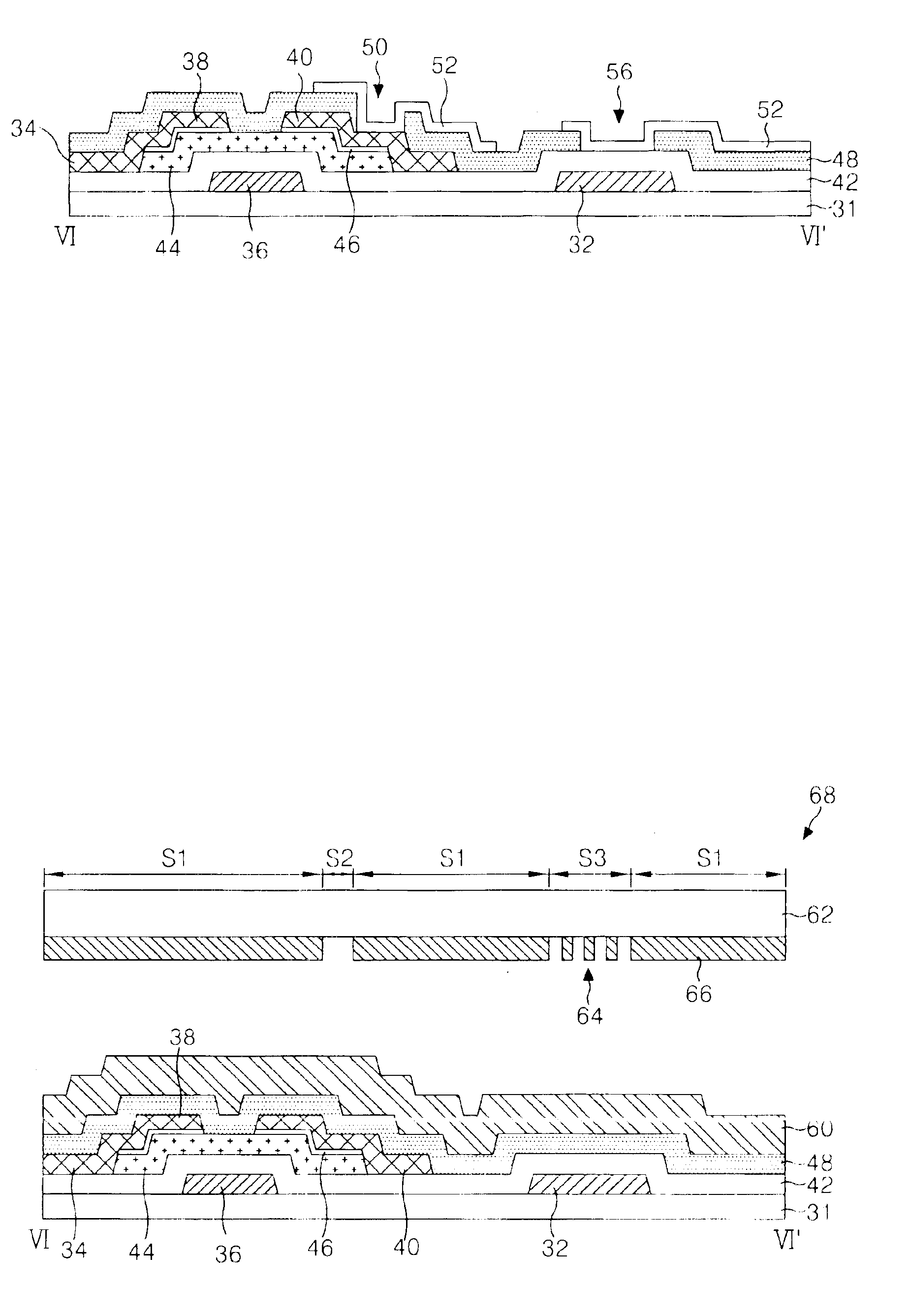
FIG. 5 is a plan view representing a liquid crystal display according to the present invention. FIG. 6 is a sectional view representing the liquid crystal display taken along the line IV-IV′ in FIG. 5.

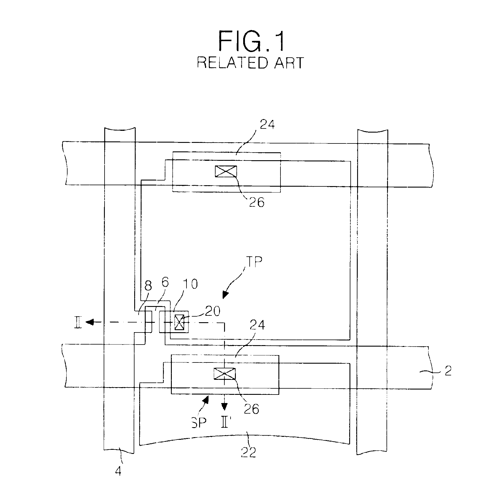
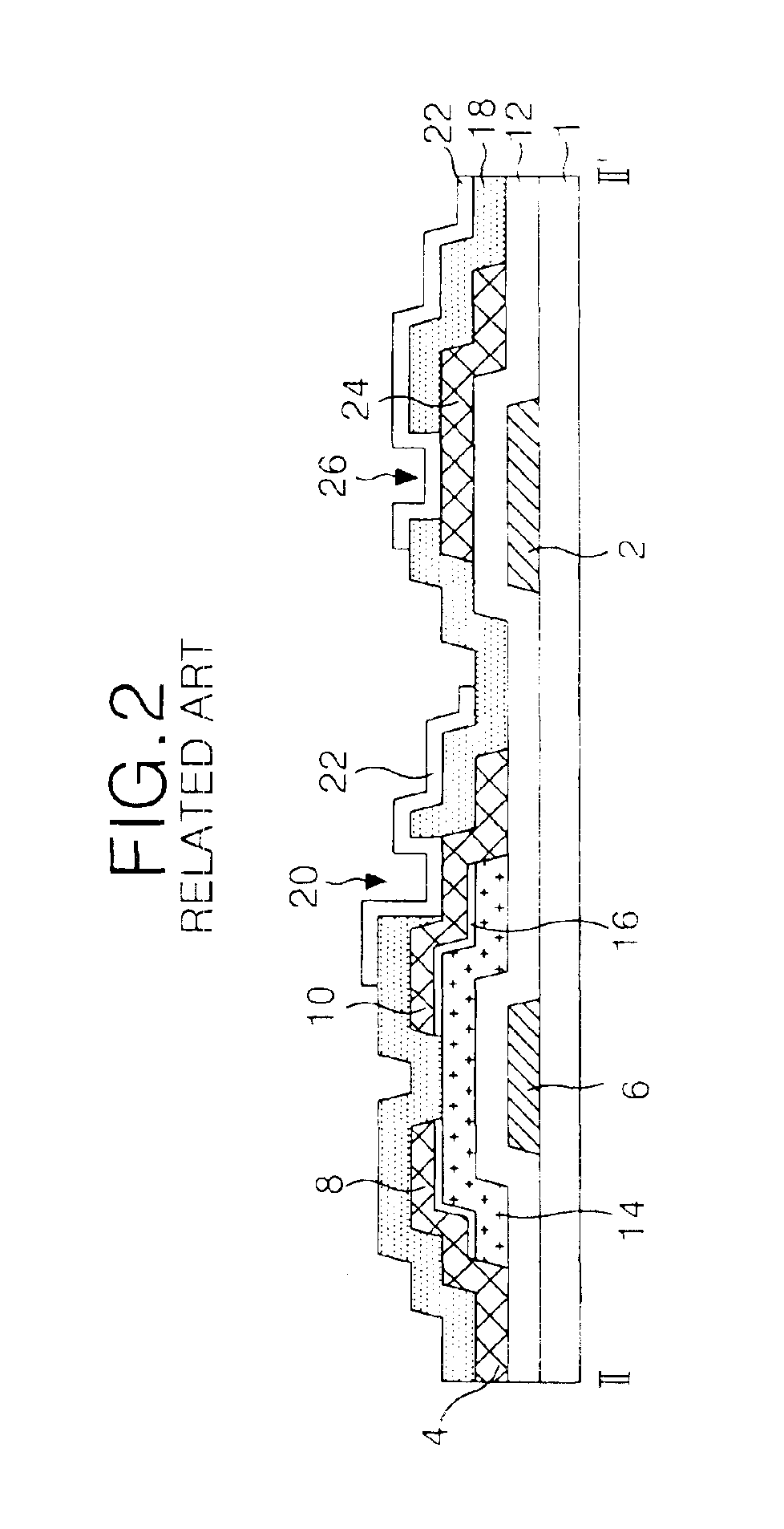
Referring to FIGS. 5 and 6, a lower substrate 31 of the liquid crystal display according to the present invention includes a TFT TP located at each intersection part of data lines 34 and gate lines 32, a pixel electrode 52 connected to a drain electrode 40, and a storage capacitor SP located at an area where the pixel electrode 52 overlaps a pre-stage gate line 32.

The TFT TP includes a gate electrode 36 connected to the gate line 32, a source electrode 38 connected to the data line 34, and a drain electrode 40 connected to the pixel electrode 52 through a drain contact hole 20. Further, the TFT TP includes semiconductor layers 44 and...


PUM

PropertyMeasurementUnit
areaaaaaaaaaaa
insulatingaaaaaaaaaa
thicknessaaaaaaaaaa

Abstract

There is disclosed a method of fabricating a liquid crystal display that is adaptive for increasing the capacitance of a storage capacitor. A method of fabricating a liquid crystal display according to an embodiment of the present invention includes forming a thin film transistor at an area where a gate line crosses a data line; forming a protective film to cover a substrate where the thin film transistor is formed; simultaneously forming a perforation hole and a contact hole by selectively eliminating the protective film using a partial exposure mask; and forming a pixel electrode contacting a gate insulating film and a drain electrode of the thin film transistor through the perforation hole and the contact hole respectively.

Description

This application claims the benefit of the Korean Patent Application No. 2002-54536, filed on Sep. 10, 2002, which is hereby incorporated by reference for all purposes as if fully set forth herein.BACKGROUND OF THE INVENTION1. Field of the InventionThe present invention relates to a liquid crystal display, and more particularly to a method of fabricating a liquid crystal display having a storage capacitor with increased capacitance.2. Description of the Related ArtGenerally, liquid crystal displays (LCD) display a picture by controlling light transmittance using electric fields. To this end, an LCD includes a liquid crystal display panel having liquid crystal cells arranged in a matrix, and a drive circuit to drive the liquid crystal display panel. The liquid crystal display panel is provided with a common electrode and pixel electrodes to apply an electric field to each liquid crystal cell. Typically, pixel electrodes are formed on a lower substrate in liquid crystal cells, whereas...

Claims


Application Information

Patent Timeline
Patent Type & Authority Patents(United States)
IPC IPC(8): H01L21/70H01L27/12H01L21/84G02F1/13H01L21/77H01L27/13
CPCH01L27/1288H01L27/1255G02F1/13
Inventor LEE, JAE GU
Owner LG DISPLAY CO LTD
Why Eureka
Try Eureka