Probe card

a technology of probe card and probe, which is applied in the direction of coupling device connection, semiconductor/solid-state device testing/measurement, instruments, etc., can solve the problems of dielectric absorption, distortion of the probe card, and inability to perform current measurement correctly, so as to reduce the waiting time of measuring, enhance the accuracy of measuring microcurrent or fluctuations, and reduce the steady-state leakage current

Inactive Publication Date: 2005-02-15
AGILENT TECH INC
View PDF7 Cites 2 Cited by
  • Summary
  • Abstract
  • Description
  • Claims
  • Application Information

AI Technical Summary

Benefits of technology

It is an object of the present invention to reduce a measuring waiting time resulted from dielectric absorption and decrease a steady-state leakage current so as to enhance accuracy of measuring microcurrents or fluctuations of them. It is another object of the present invention to reduce variations of properties of each pin or each probe card.

Problems solved by technology

Major problems on developing testing devices with such high performance include leakage current between adjoining electric wires for connecting a testing device and a semiconductor to be measured and dielectric absorption occurring between such wires and dielectrics in a probe card substrate.
For example, the problem of dielectric absorption occurs due to dielectric absorption properties (absorption current) of the dielectric used as the probe card substrate.
Therefore, even if a predetermined voltage is applied to a semiconductor wafer for current measurement, the current measurement can not be performed correctly for a certain time period and a waiting time is necessary until the current flow becomes stabilized.
This is one of important problems in case of reducing the time required for the microcurrent measurement.
One problem in such a method is that a distortion tends to occur in the probe card as the number of through-holes is increases, and that the physical strength of the card degrades in or near the region of the through-holes.
Even if the number of the through-holes is increased regardless of manufacturing difficulties and cost elevation, some leakage current through the dielectric between these through-holes still remains as a problem, and a dielectric loss can not be reduced to a desired level as a higher level of measuring accuracy is required.
Therefore, even if the manufacturing process control is improved sufficiently, such variations in the dielectric and current leakage properties of each wire for each probe card would limit the accuracy of current measurements.

Method used


Image

  • Probe card
  • Probe card
  • Probe card

Examples


Embodiment Construction

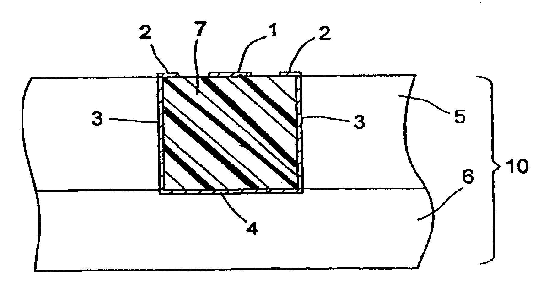
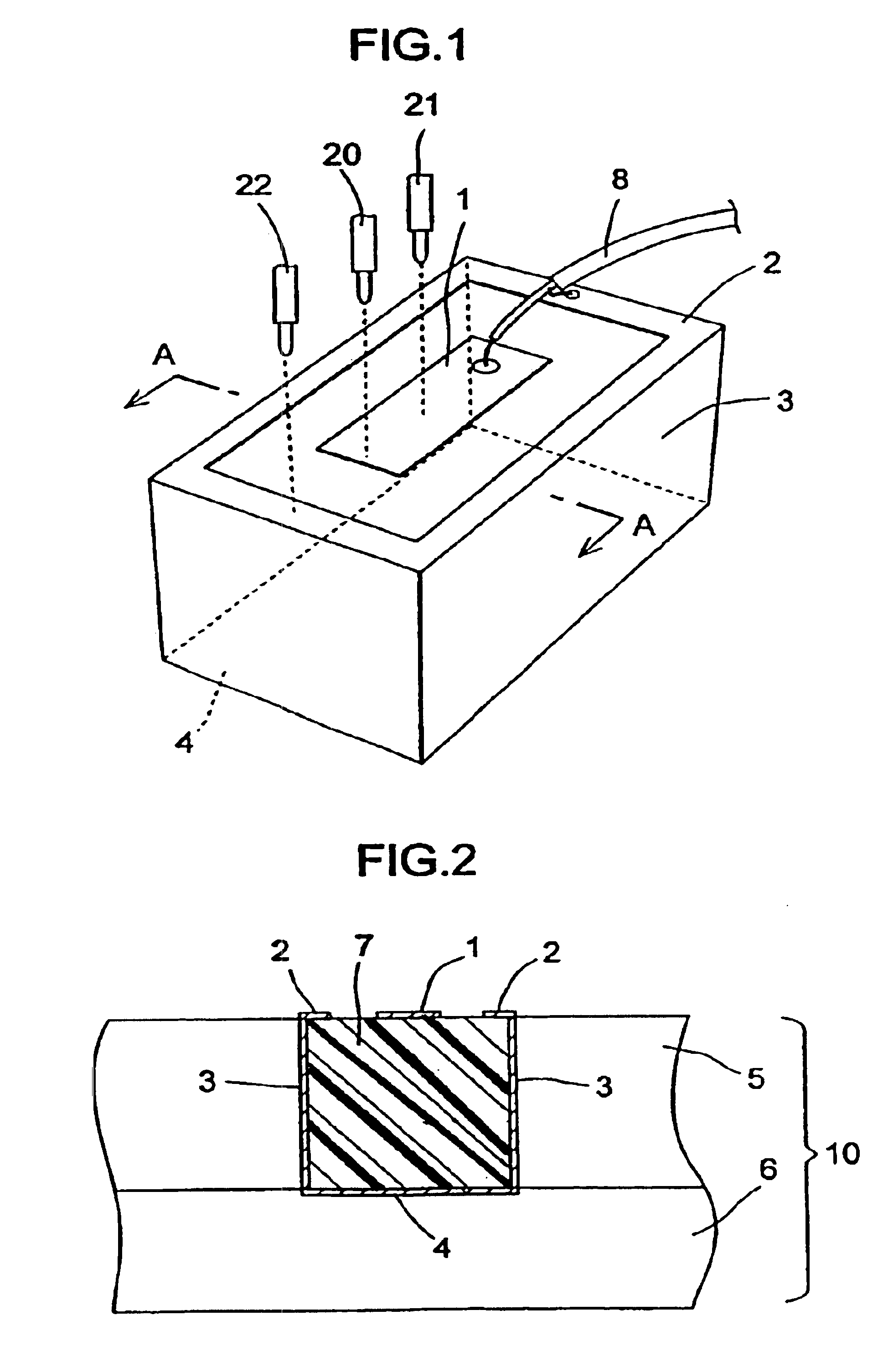
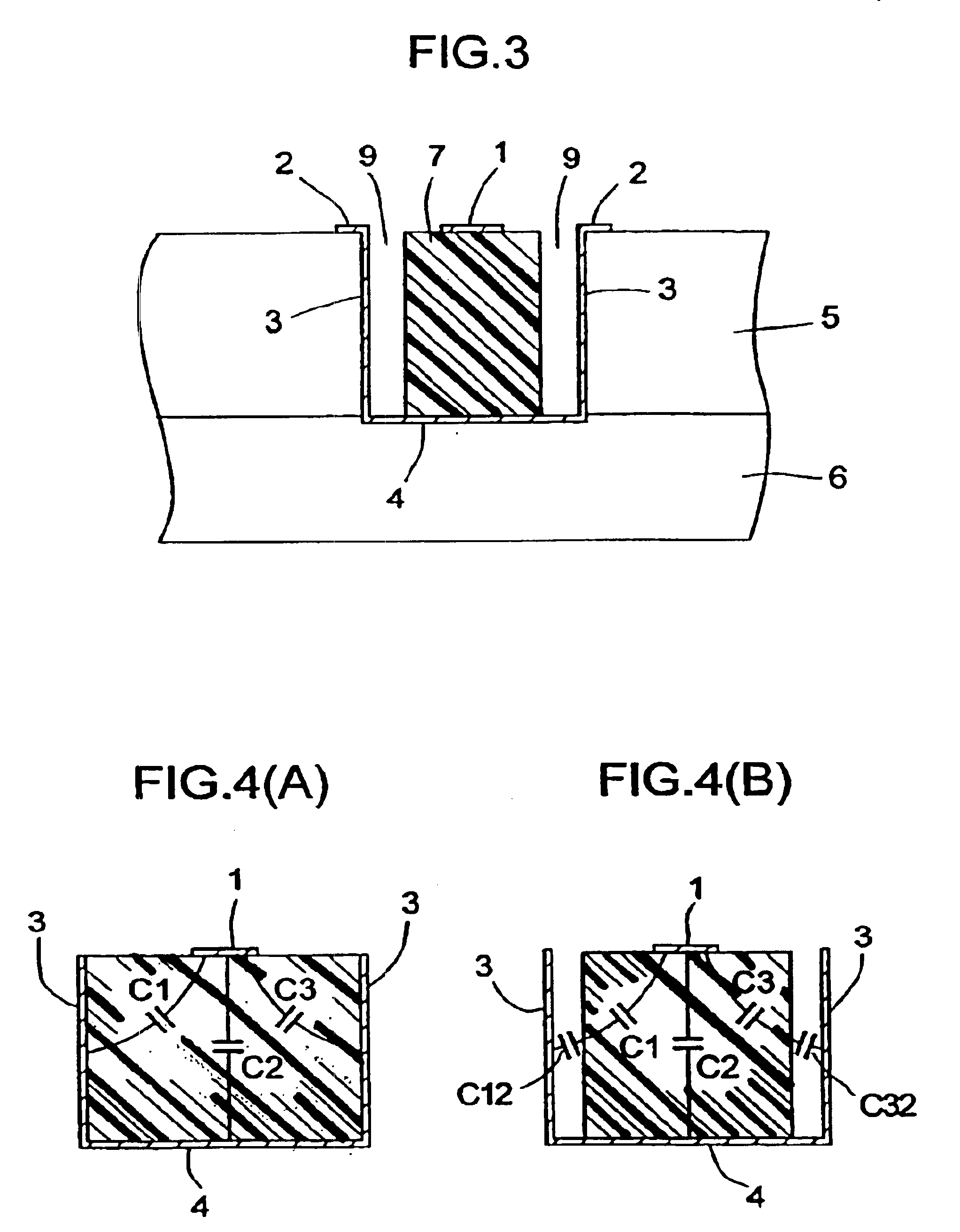
Several embodiments of the present invention will be described with reference to FIGS. 1 to 9. FIG. 1 shows a fundamental embodiment of the present invention. In the same drawing surrounding substrate portions are eliminated to show external connection terminal 1 and a conductor material, including upper guard pattern 2, side conductors 3, and bottom conductor 4 placed around it. The conductor material 2, 3, 4 is electrically connected and equipotential to one another. On the substrate, the external connection terminal 1 and the upper guard pattern 2 surrounding the terminal 1 can be seen, both of which are composed of conductor. Over the external connection terminal 1 and the upper guard pattern 2, three contact pin members 20, 21, 22 projecting from a test head of a semiconductor measuring device are positioned so as to contact with their corresponding targets. In this embodiment, the contact pin member 20 is a so-called “force” terminal for applying a voltage and measuring a curr...


PUM


Abstract

The present invention provides a probe card comprising a substrate and an external connection terminal located on substrate, wherein external connection terminal 1 is separated from a body of substrate by conductors attached to the substrate, whereby the waiting time due to dielectric absorption can be constantly shortened, and the steady-state leakage current can be stably reduced, thereby enhancing the accuracy of measuring microcurrents and determining microcurrent fluctuations for semiconductor wafer testing devices.

Description

BACKGROUND OF THE INVENTION1. Field of the InventionThe present invention relates to a probe card for connecting a wafer to be measured with a measuring device in a semiconductor wafer testing device.2. Description of the Related ArtMarked progress has been seen in the recent semiconductor manufacturing technology, including the progress of fine processing technology required for high density integration. For high density implementation as well as for suppression of heat generation and downsizing each elements, the current and voltage required for operation in the semiconductor devices are reduced year by year. Thus, the importance of microcurrent measurement has been recognized, and higher accuracies in microcurrent measurement are required in probe cards for connecting measuring devices and wafers.Such a requirement is also present in the wafer process control testing. As a conventional testing method for process control, measurement chips referred to as TEG (Test Element Group) a...

Claims


Application Information

Patent Timeline
Patent Type & Authority Patents(United States)
IPC IPC(8): G01R1/067G01R3/00G01R1/073H05K1/02H01L21/66
CPCG01R1/07307H05K1/0268G01R3/00G01R1/07342
Inventor IWASAKI, YUKOH
Owner AGILENT TECH INC
Why Eureka
Try Eureka