Vertical nano-size transistor using carbon nanotubes and manufacturing method thereof

a carbon nanotube and nano-sized technology, applied in nanoinformatics, instruments, coatings, etc., can solve the problems of limited processing precision and integration, difficulty in reducing the size of switching devices, and difficulty in controlling individual carbon nanotubes

Inactive Publication Date: 2005-02-15
SAMSUNG ELECTRONICS CO LTD
View PDF15 Cites 69 Cited by
  • Summary
  • Abstract
  • Description
  • Claims
  • Application Information

AI Technical Summary

Benefits of technology

In order to solve the aforementioned problems, it is a feature of an embodiment of the present invention to provide by vertical growth and selective deposition a vertical transistor ranging in size from several tens of nanometers to one micron using tera-bit scale carbon nanotubes as channels where each of the carbon nanotubes has a diameter of several nanometers and is grown on a nonconductive substrate having nano-sized holes. The lower and upper parts of each carbon nanotube are connected to a source and a drain, respectively, with a gate interposed between the source and the drain for performing switching.

Problems solved by technology

A problem arising from forming an impurity diffusion region and an isolation region on a silicon substrate is that there are limits in processing precision and integration.
A result of the limitations imposed by forming an impurity diffusion region and an isolation region on a silicon substrate is the difficulty to decrease the size of the switching device.
However, the proposed device still has a horizontal structure similar to that of other conventional switching devices making it quite difficult to control the individual carbon nanotubes.
As a result, it is difficult to achieve high-density integration of switching devices using carbon nanotubes.

Method used


Image

  • Vertical nano-size transistor using carbon nanotubes and manufacturing method thereof
  • Vertical nano-size transistor using carbon nanotubes and manufacturing method thereof
  • Vertical nano-size transistor using carbon nanotubes and manufacturing method thereof

Examples


first embodiment

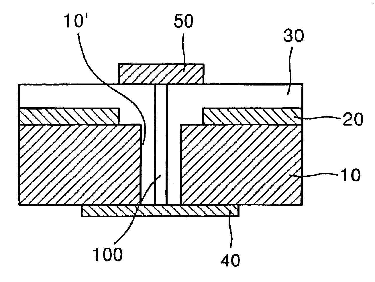
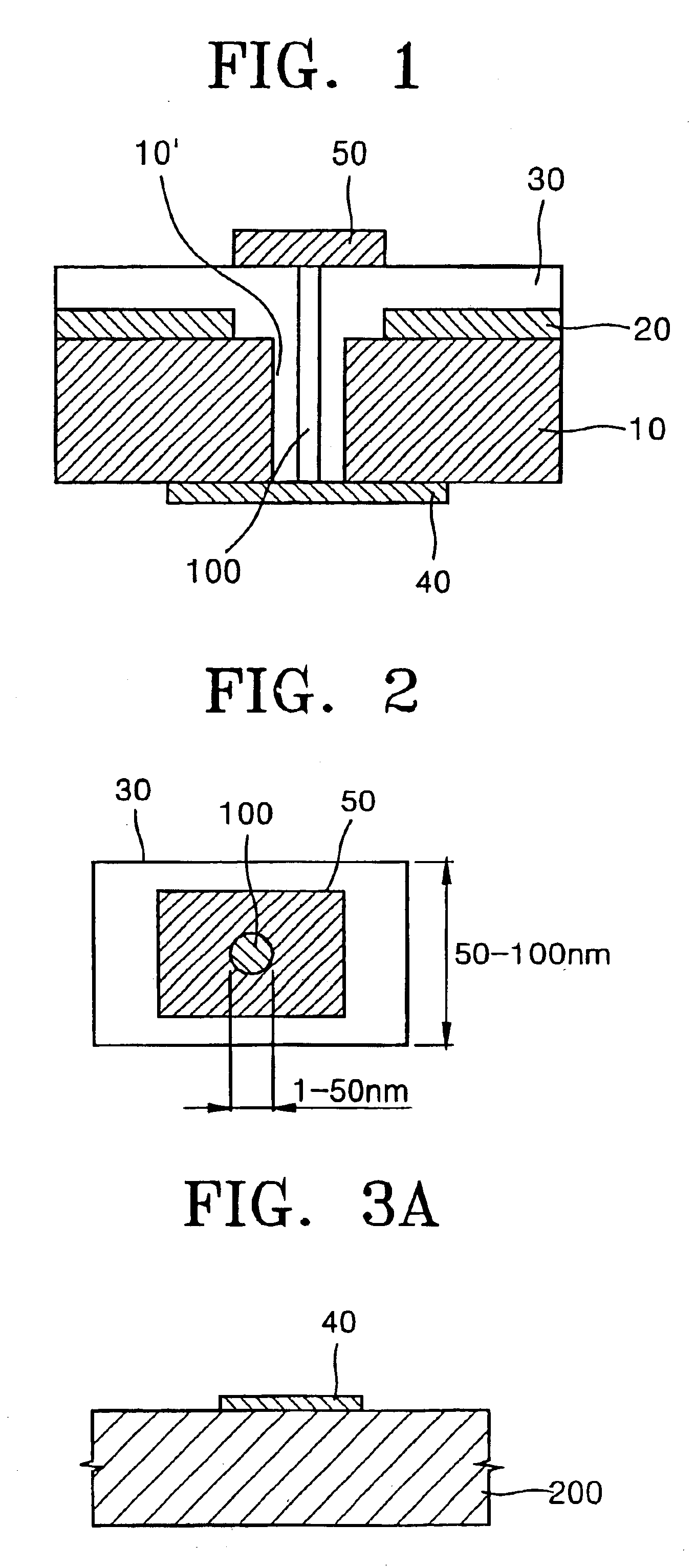
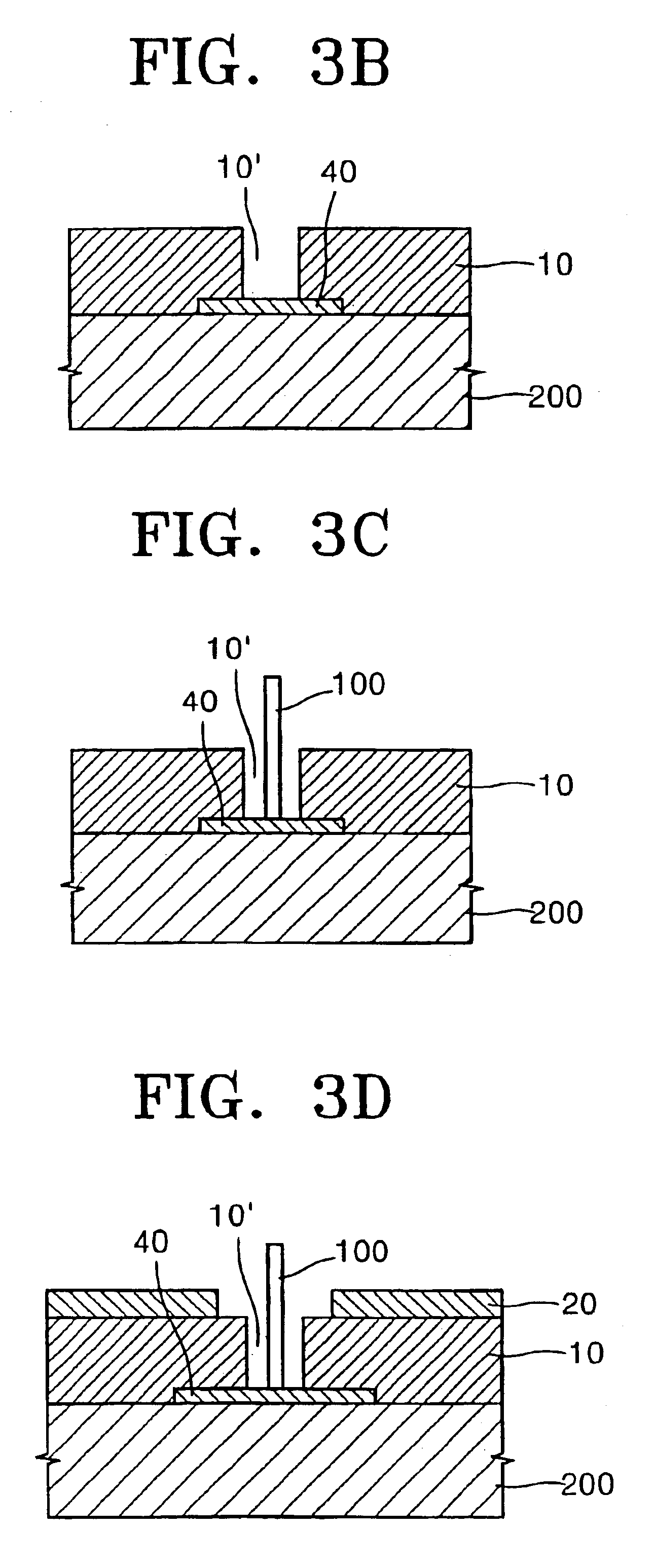
A vertical nano-sized transistor using carbon nanotubes according to the present invention will now be explained. As shown in FIG. 1, a unit cell of a vertically aligned carbon nanotube transistor is constructed as follows.

First, a carbon nanotube 100 is arranged on a nonconductor substrate 10 having a nano-sized hole 10′ formed by vertical growth and selective deposition. A gate 20 is formed on the nonconductor substrate 10 in the vicinity of the carbon nanotube 100, and a nonconductor film 30 is deposited thereon to fill the hole 10′. Here, an insulating film such as alumina is used as the nonconductor substrate 10, and the size of the hole and the distance between adjacent holes can be adjusted to dimensions of several nanometers. In such a manner, high-density integration, that is, tera-bit scale integration, can be achieved.

In other words, the vertically grown carbon nanotube 100 having a nano-sized diameter is used as a channel and is constructed such that the lower and upper ...


PUM

PropertyMeasurementUnit
areaaaaaaaaaaa
sizeaaaaaaaaaa
areaaaaaaaaaaa

Abstract

The present invention provide a vertical nano-sized transistor using carbon nanotubes capable of achieving high-density integration, that is, tera-bit scale integration, and a manufacturing method thereof, wherein in the vertical nano-sized transistor using carbon nanotubes, holes having diameters of several nanometers are formed in an insulating layer and are spaced at intervals of several nanometers. Carbon nanotubes are vertically aligned in the nano-sized holes by chemical vapor deposition, electrophoresis or mechanical compression to be used as channels. A gate is formed in the vicinity of the carbon nanotubes using an ordinary semiconductor manufacturing method, and then a source and a drain are formed at lower and upper parts of each of the carbon nanotubes thereby fabricating the vertical nano-sized transistor having an electrically switching characteristic.

Description

BACKGROUND OF THE INVENTION1. Field of the InventionThe present invention relates to a vertical nano-sized transistor and a method for manufacturing the same. More specifically, the present invention relates to a vertical nano-sized transistor using carbon nanotubes capable of achieving high-density, or tera-bit scale, integration and a method for manufacturing the same.2. Description of the Related ArtA switching device fabricated using a conventional silicon substrate is generally constructed such that an impurity diffusion region, an isolation region and a channel region are horizontally connected on the silicon substrate. An integrated circuit consisting of multiple switching devices is constructed such that the individual switching devices are horizontally arranged to be highly integrated. A problem arising from forming an impurity diffusion region and an isolation region on a silicon substrate is that there are limits in processing precision and integration. A result of the li...

Claims


Application Information

Patent Timeline
Patent Type & Authority Patents(United States)
IPC IPC(8): G11C13/02H01L21/02H01L29/66H01L21/335H01L29/775H01L51/30H01L51/05B82B1/00B82B3/00C23C16/26H01L21/336H01L21/8234H01L29/06H01L29/732H01L29/74H01L29/76H01L29/78H01L29/786H01L35/24
CPCB82Y10/00G11C13/025H01L29/66439H01L29/775H01L51/0048H01L51/0508G11C2213/17Y10S977/708H01L51/057Y10S977/742Y10S977/843Y10S977/723Y10S977/938H10K85/221H10K10/46H10K10/491H01L29/732
Inventor CHOI, WON-BONGLEE, JO-WONLEE
Owner SAMSUNG ELECTRONICS CO LTD
Why Eureka
Try Eureka