Silicon carbide having low dielectric constant

a silicon carbide and dielectric constant technology, applied in the direction of basic electric elements, semiconductor/solid-state device manufacturing, electric apparatus, etc., can solve the problems of resistance-capacitance (rc) coupling and the resulting rc delay becoming more of a problem

Inactive Publication Date: 2005-02-15
NOVELLUS SYSTEMS
View PDF9 Cites 65 Cited by
  • Summary
  • Abstract
  • Description
  • Claims
  • Application Information

AI Technical Summary

Benefits of technology

[0011]In another aspect, flowing a low-k precursor comprises flowing ETMS gas and an inert gas into the reaction chamber. In another aspect, the ETMS/inert flow rate ratio is in a range of about from 2/1 to 1/10. In still another aspect, flowing a low-k precursor comprises flowing ETMS gas and a doping gas into the reaction chamber. In another aspect, the ETMS/doping flow rate ratio is in a range of about from 2/1 to 1/20. In still another aspect, flowing ETMS gas and a doping gas into the reaction chamber comprises flowing ETMS gas and CO2 gas at a ETMS/CO2 flow rate ratio in a range of about from 1/2 to 1/20, preferably at a ETMS/CO2 flow rate ratio in a range of about from 1/4 to 1/10.
[0012]In another aspect, forming a plasma comprises maintaining a pressure in the reaction chamber in a range of about from 1 Torr to 9 Torr, and applying HF RF power to the reaction chamber at a frequency in a range of about from 1 MHz to 100 MHz and at a pow

Problems solved by technology

As the density of integrated circuits increases and feature sizes become smaller, re

Method used


Image

  • Silicon carbide having low dielectric constant
  • Silicon carbide having low dielectric constant
  • Silicon carbide having low dielectric constant

Examples


example 1

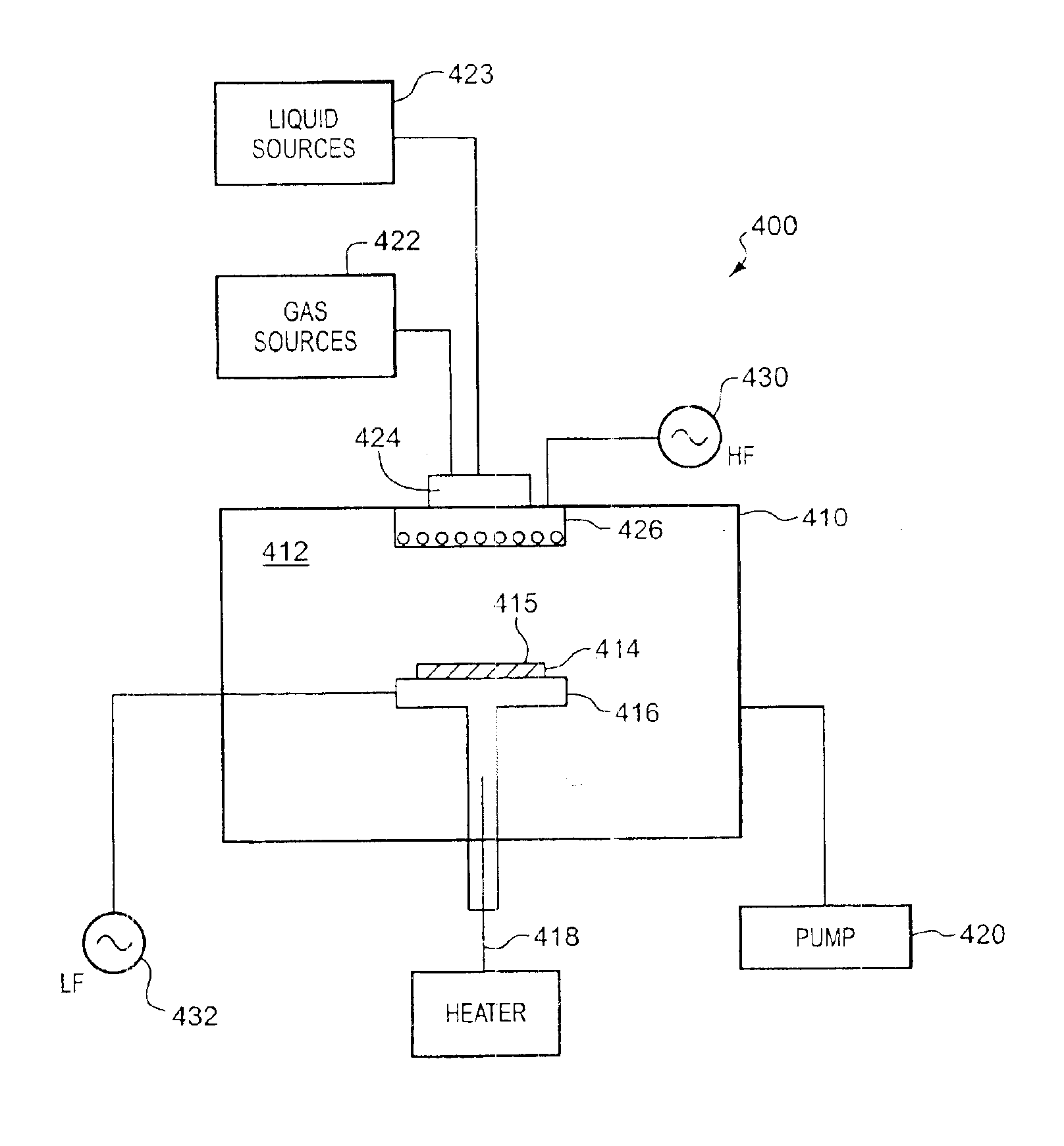
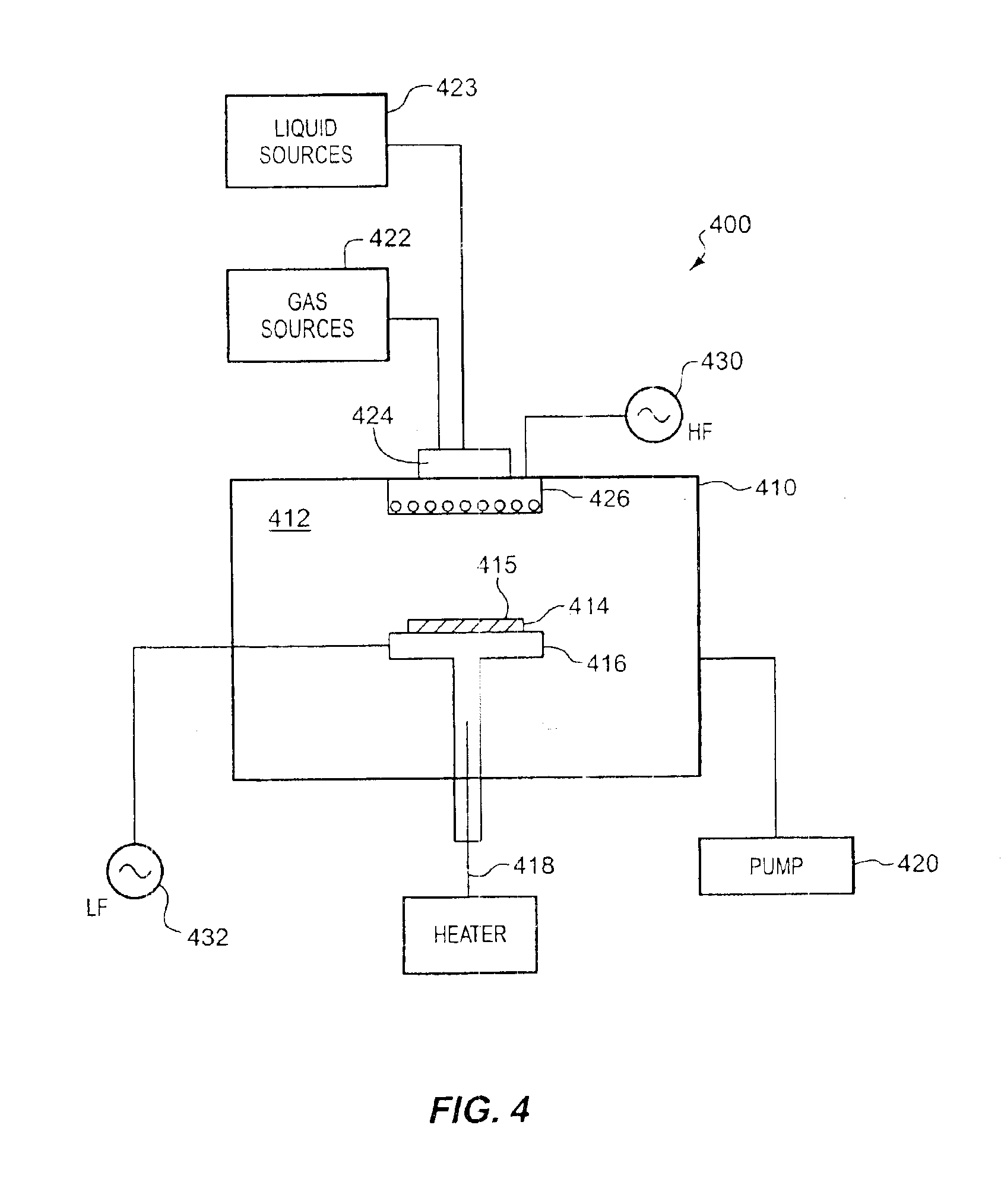
[0061]A series of exemplary low-k SiC films was fabricated using a PECVD method in accordance with the invention using the low-k precursor reactant ETMS. Each low-k SiC film was deposited on a 200 mm silicon semiconductor wafer substrate in a Novellus “Sequel” model, 6-station dual-frequency PECVD apparatus. The substrate surface before processing comprised monocrystalline silicon. The low-k SiC was deposited at a wafer temperature of about 400° C. Pure low-k precursor ETMS reactant gas was flowed into the process reaction chamber at a flow rate of 500 sccm. Process conditions between example wafers were varied to determine the effect of various operating parameters on film characteristics.

[0062]Inert helium gas was mixed with the ETMS precursor gas in a gas mixer and the gaseous reactant mixture was introduced into the reaction chamber at a constant flow rate. The flow rate of helium gas varied in a range of about from 1000 sccm to 3000 sccm. HF RF power was applied to the showerhe...

example 2

[0070]A series of doped, low-k SiC films was deposited on silicon substrates using conditions similar to those in Example 1, except carbon dioxide doping gas, CO2, was introduced into the reaction chamber instead of inert helium gas. Operating conditions and measured film characteristics are presented in Table 4, below.

TABLE 4Rec-ipeNum-ETMSCO2PresHFLF    k (1Si—C / ber(Sccm)(Sccm)(Torr)(W)(W)RI   hr)Si—O31500150026003001.636  3.281.1232500300026003001.6553  3.530.8633500450026003001.6672  3.680.7434500150046003001.5707  2.931.1035500300046003001.5782  3.100.8836500450046003001.5834  3.190.7837500150026006001.6539  3.450.9638500300026006001.6721  3.760.7439500450026006001.6837  3.920.62

[0071]The films had a thickness in a range of about 75 nm to 79 nm. The stability of the dielectric constant, k, of the films was tested. The measured k-values at one hour after formation of the films was in a range of about 2.9 to 3.9. The dielectric constant was measured right after deposition and aft...

example 3

[0074]A series of exemplary low-k SiC films was fabricated using a PECVD method in accordance with the invention using the low-k precursor reactant HMDS. Each low-k SiC film was deposited on a 200 mm silicon semiconductor wafer substrate in a Novellus “Sequel” model, 6-station dual-frequency PECVD apparatus. The substrate surface before processing comprised monocrystalline silicon. The low-k SiC was deposited at a wafer temperature of about 400° C. Pure low-k precursor HMDS reactant liquid was injected into the mixing bowl at a flow rate in a range of about 1.0 ccm to 3.0 ccm. The liquid HMDS was gasified in the mixing bowl, where it was mixed with CO2 doping gas. The constant flow rate of CO2 doping gas varied between wafers in a range of about from 2000 sccm to 5000 sccm. The resulting reactant gas mixture was fed into the CVD reaction chamber. HF RF power was applied to the showerhead at a frequency of 13.56 MHz, and the HF power was varied in a range of about from 400 Watts to 7...


PUM


Abstract

A low-k precursor reactant compound containing silicon and carbon atoms is flowed into a CVD reaction chamber. High-frequency radio-frequency power is applied to form a plasma. Preferably, the reaction chamber is part of a dual-frequency PECVD apparatus, and low-frequency radio-frequency power is applied to the reaction chamber. Reactive components formed in the plasma react to form low-dielectric-constant silicon carbide (SiC) on a substrate surface. A low-k precursor is characterized by one of: a silicon atom and a carbon—carbon triple bond; a silicon atom and a carbon—carbon double bond; a silicon—silicon bond; or a silicon atom and a tertiary carbon group.

Description

FIELD OF THE INVENTION[0002]The invention is related to the field of barrier etch stop and insulator layers in integrated circuits, in particular, to silicon carbide layers having a low dielectric constant.BACKGROUND OF THE INVENTION[0003]Statement of the Problem[0004]Conventional semiconductor devices typically comprise a semiconductor substrate, usually of doped monocrystalline silicon, and a plurality of sequentially formed intermetal dielectric layers and electrically conductive patterns. An integrated circuit contains a plurality of patterns of conductive lines separated by interwiring spacings, and a plurality of interconnect lines, such as bus lines, bit lines, word lines, and logic interconnect lines. Typically, the conductive patterns of vertically spaced metallization levels are electrically interconnected by vertically oriented conductive plugs filling via holes formed in the intermetal dielectric layer separating the metallization levels, while other conductive plugs fil...

Claims


Application Information

Patent Timeline
IPC IPC(8): H01L21/70H01L21/02H01L21/314H01L21/768
CPCH01L21/76829H01L21/3148H01L21/02274H01L21/02167H01L21/02216
Inventor TANG, XINGYUANFU, HAIYING
Owner NOVELLUS SYSTEMS
Why Eureka
Try Eureka