

Method of fabricating substrates, in particular for optics, electronics or optoelectronics
a substrate and electronics technology, applied in the field of optics, electronics or optoelectronics, can solve the problems of long polishing time, long preparation time, and high cost of above-mentioned steps, and achieve the effect of minimizing the loss of starting materials
- Summary
- Abstract
- Description
- Claims
- Application Information
AI Technical Summary
Benefits of technology
Problems solved by technology
Method used
Image

Examples
example 1
[0068]A monocrystalline silicon carbide ingot 10 was used. Its periphery had a polycrystalline gangue inherent to the growth method employed. The ingot had a diameter of about 60 mm and a length on the order of 50 mm. Depending on the envisaged applications, the ingot could be of polytype 4H or 6H, using the denominations employed by the skilled person.
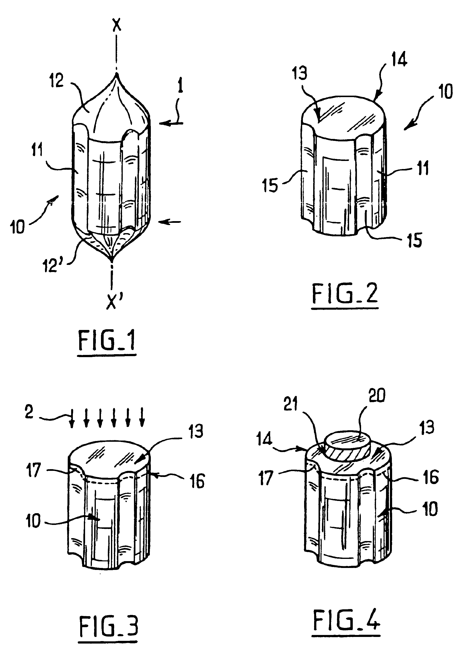
[0069]The ingot underwent cutting and lapping operations to result in an ingot as illustrated in FIG. 2, and a polishing finishing step was used. Preferably, prior to the polishing finishing step, a chemical attack step was carried out to remove a zone damaged during the mechanical material removal steps. Typically, 10 μm of material was removed during this chemical attack step.
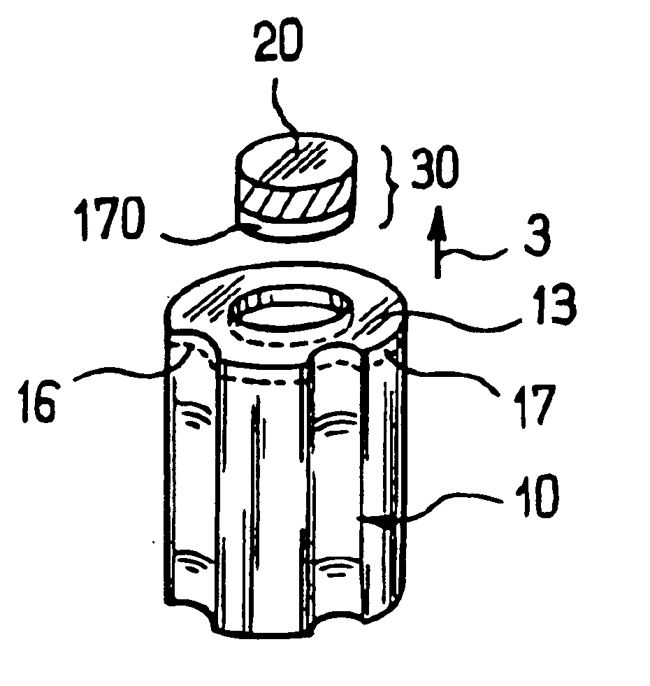
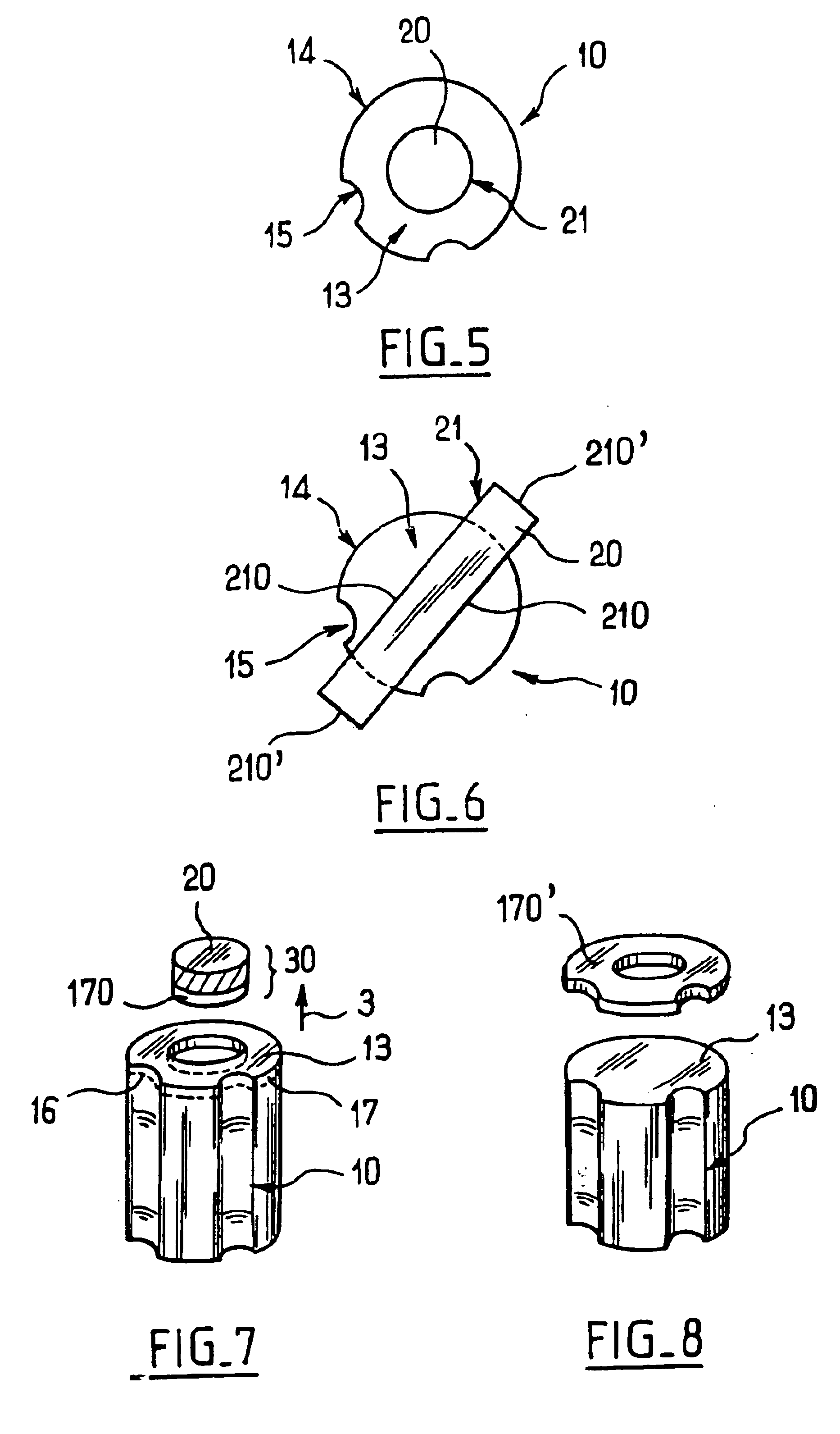
[0070]Depending on the polytype, the surface 13 of the ingot will be selected to be substantially parallel to a crystallographic plane (polytype 6H, on-axis) or deliberately out of orientation by a few degrees (as is routine in the case of polytype 4H, for exam...
example 2
[0078]This example reproduced Example 1, but differed in that the ingot 10 was an ingot of monocrystalline silicon. This ingot had a diameter of slightly more than 300 mm, or about 310 mm, a crystallographic orientation and a length of 1.20 m, ignoring the conical ends. It could be obtained using any known technique such as CZ (CZOCHALSKI) pulling.
[0079]As shown in FIG. 2, this ingot 10 also underwent a cutting operation aimed at removing the conical ends 12, 12′. The ingot also underwent a turning operation to form a circular cylinder with a diameter of about 300 mm, with a diameter tolerance that was greater than the normal standards fixing tolerances for the diameter of substrates. A diameter of 302 mm±1 mm, and thus slightly irregular, was obtained.
[0080]In contrast to the preceding example, this ingot 10 underwent segmenting to define six segments of ingot each with a length of the order of 20 cm. Each ingot segment was then lapped, and its ends were polished to obtain six seg...
example 3
[0087]Example 3 reproduces Example 2 but the ingot 10 was cut into twenty-four segments each with a thickness of the order of 50 mm.
[0088]In this example, the loss of material linked to the cutting, grinding and polishing operations was higher than in Example 2 in which only six segments were cut. In contrast, more segments were obtained on which it was possible to operate in parallel.
PUM
| Property | Measurement | Unit |
|---|---|---|
| Thickness | aaaaa | aaaaa |
| Pressure | aaaaa | aaaaa |
| Flexibility | aaaaa | aaaaa |
Abstract
Description
Claims
Application Information