
Semiconductor device and method of producing the same

Inactive Publication Date: 2005-02-22
SANYO ELECTRIC CO LTD
View PDF22 Cites 5 Cited by
  • Summary
  • Abstract
  • Description
  • Claims
  • Application Information

AI Technical Summary

Benefits of technology

The present invention is made so as to solve the foregoing problems of the related art, and it is an object of the present invention to provide a semiconductor device having excellent characteristics and a method of producing such a semiconductor device, in which projections generated on a semiconductor film are eliminated to planarize the film surface.
In accordance with the present invention, a method of producing a semiconductor device comprises the steps of forming a non-crystal semiconductor film on a substrate; heating said non-crystal semiconductor film: and eliminating projections generated by said heating on said non-crystal semiconductor film using a physical elimination method.
Also, in accordance with another aspect of the present invention, a semiconductor device comprises a substrate and a non-crystal semiconductor film formed on said substrate, wherein said non-crystal semiconductor film has a planar surface by eliminating, using ion beam irradiation, projections generated on said non-crystal semiconductor film due to heating of said film.
According to the present invention, projections generated on the surface of p-si (non-crystal semiconductor) film can be effectively eliminated such that the surface can be planarized using the ion milling method, allowing a semiconductor device having excellent characteristics can be obtained.

Problems solved by technology

TFTs produced in the above-described manner suffer from problems.
When the thickness of the p-Si film 13 is approximately 400 Å, for example, the projection may be as thick as 400 Å. This leads to a disadvantage that sufficient insulation may not be achieved between the p-Si film 13 and the gate electrode 15, or that, when the height of projection 100 is larger than the thickness of the gate insulating film 14, there is a short circuit between the p-Si film 13 and the gate electrode 15.
Further, concentration of electric field in the projection 100 due to applied voltages causes dielectric breakdown, which also results in possibility of short circuit between the p-Si film 13 and the gate electrode 15.
This results in a TFT having non-uniform characteristics.
When such a TFT is employed in a display device such as a liquid crystal display, there is a possibility that variations in display characteristics are caused within the display screen.

Method used


Image

  • Semiconductor device and method of producing the same
  • Semiconductor device and method of producing the same
  • Semiconductor device and method of producing the same

Examples


Embodiment Construction

A preferred embodiment of the present invention will be described in further detail with reference to the accompanying drawings.

An example will be described where a method of producing a semiconductor device according to the present invention is adopted for a liquid crystal display comprising TFTs.

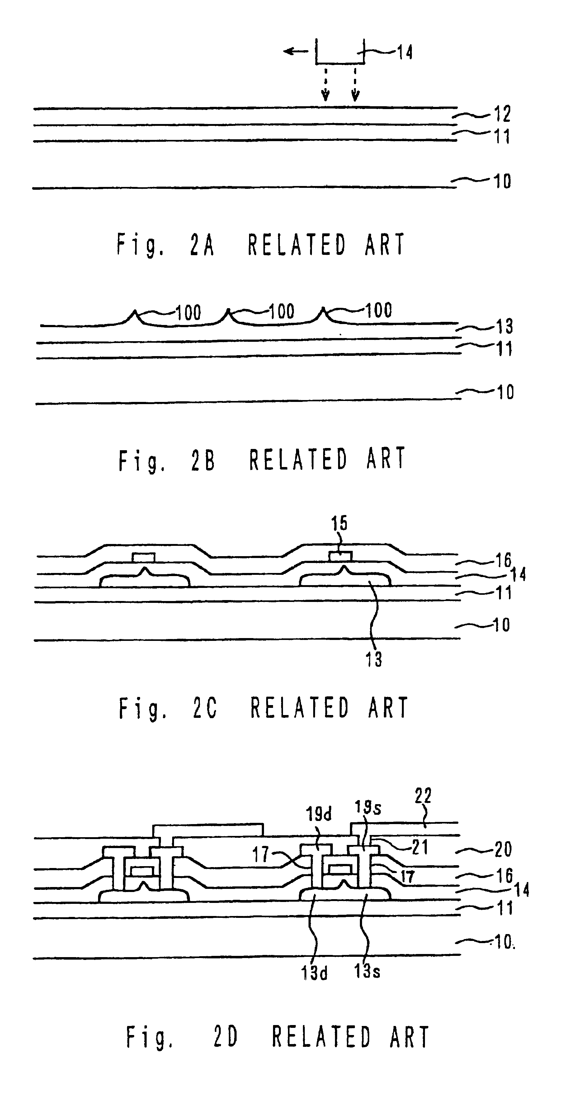
FIGS. 3A to 3E are cross sectional views for explaining the producing processes of a TFT according to the present invention, and FIG. 4 is a cross sectional view of a liquid crystal display.

Step 1 (FIG. 3A):

On an insulating substrate 10 composed of a glass, a quartz glass or the like, an insulating film 11 composed of a single SiO2 film or of an SiN film and an SiO2 film is formed using the CVD method or the like, for the purpose of preventing impurities including sodium ions in the insulating substrate from entering a semiconductor film (p-Si film) formed thereon. When a nonalkaline glass substrate or the like which can be guaranteed to remain free of impurities is employed, formation of ...


PUM


Abstract

An a-Si film (12) formed on an insulating substrate (10) is irradiated with a laser so that the a-Si film (12) is fused and recrystallized to form a p-Si film (13). Projections (100) generated on the p-Si film (13) at this stage are eliminated by irradiation of ion beams at the incident angle of 60° to 90° using an ion milling method to planarize the surface of the p-Si film (13), thereby creating sufficient insulation between the p-Si film (13) and gate electrodes (15).

Description

BACKGROUND OF THE INVENTION1. Field of the InventionThis invention relates to a semiconductor device and a method of producing the same, and more specifically to a semiconductor device comprising a semiconductor film having a planar surface and a method of producing such a semiconductor device.2. Description of Related ArtA method of producing a thin film transistor (hereinafter referred to as a “TFT”) will be described.FIG. 1 depicts the condition of the surface of a polycrystallized silicon film. FIGS. 2A to 2D respectively depict cross sectional views taken along line A—A of FIG. 1 for showing production processes of a conventional TFT.Step 1 (FIG. 2A):On an insulating substrate 10 composed of a glass, a silica glass, or the like, an insulating film 11 composed of a single SiO2 film or of an SiN film and an SiO2 film is formed, and an amorphous silicon film (hereinafter referred to as an “a-si film”) 12 is further formed thereon using a CVD method.Step 2 (FIG. 2B):The a-Si film 1...

Claims


Application Information

Patent Timeline
IPC IPC(8): H01L21/70H01L21/20H01L21/02H01L29/786H01L29/66H01L21/336H01L21/84H01L21/302H01L21/3065H01L21/3205H01L21/321H01L21/77H01L29/04
CPCH01L21/2026H01L21/32055H01L21/32115H01L27/1285H01L29/66757H01L29/78636H01L29/04H01L21/02422H01L21/02488H01L21/02532H01L21/02686H01L21/302H01L21/02595
Inventor MORIMOTO, YOSHIHIROYONEDA, KIYOSHI
Owner SANYO ELECTRIC CO LTD
Features
  • Generate Ideas
  • Intellectual Property
  • Life Sciences
  • Materials
  • Tech Scout
  • Unparalleled Data Quality
  • Higher Quality Content
  • 60% Fewer Hallucinations
Learn More