Method for manufacturing a silicon carbide semiconductor element

a semiconductor element and manufacturing method technology, applied in semiconductor devices, semiconductor/solid-state device testing/measurement, electrical apparatus, etc., can solve the problems of difficult to remove resists, physical properties of carbide semiconductors, difficult control dimensions, etc., to reduce breakdown voltage, improve breakdown voltage, and reduce breakdown voltage

Inactive Publication Date: 2017-09-12
FUJI ELECTRIC CO LTD
View PDF24 Cites 0 Cited by
  • Summary
  • Abstract
  • Description
  • Claims
  • Application Information

AI Technical Summary

Benefits of technology

[0020]According to the above-mentioned structure, dry etching is performed on the ion implantation mask formed on the silicon carbide substrate to form the residual portion, which has a predetermined thickness and is made of the same material as the mask portion, in the bottom of the opening of the ion implantation portion. Therefore, even when dry etching is performed, the surface of the silicon carbide substrate is not damaged and can be planarized. As a result, a reduction in the breakdown voltage is suppressed and the breakdown voltage can be improved.
[0021]According to the invention, it is possible to obtain a silicon carbide semiconductor element which can prevent the damage of the surface of the silicon carbide semiconductor when the ion implantation mask is formed, easily form the opening portion of the ion implantation mask with high accuracy, and improve the breakdown voltage.

Problems solved by technology

However, the surface of the silicon carbide semiconductor is physically or electrically damaged due to plasma or active species generated during etching, which causes breakdown when a high voltage is applied.
However, the technique using photoresist for the ion implantation mask has the following issues 1 to 3.
In this case, since the resist is shrunk, it is difficult to control dimensions.
3. The resist closely adheres to the substrate due to a high temperature or exposure to plasma, which makes it difficult to remove the resist.

Method used


Image

  • Method for manufacturing a silicon carbide semiconductor element
  • Method for manufacturing a silicon carbide semiconductor element
  • Method for manufacturing a silicon carbide semiconductor element

Examples


embodiment 1

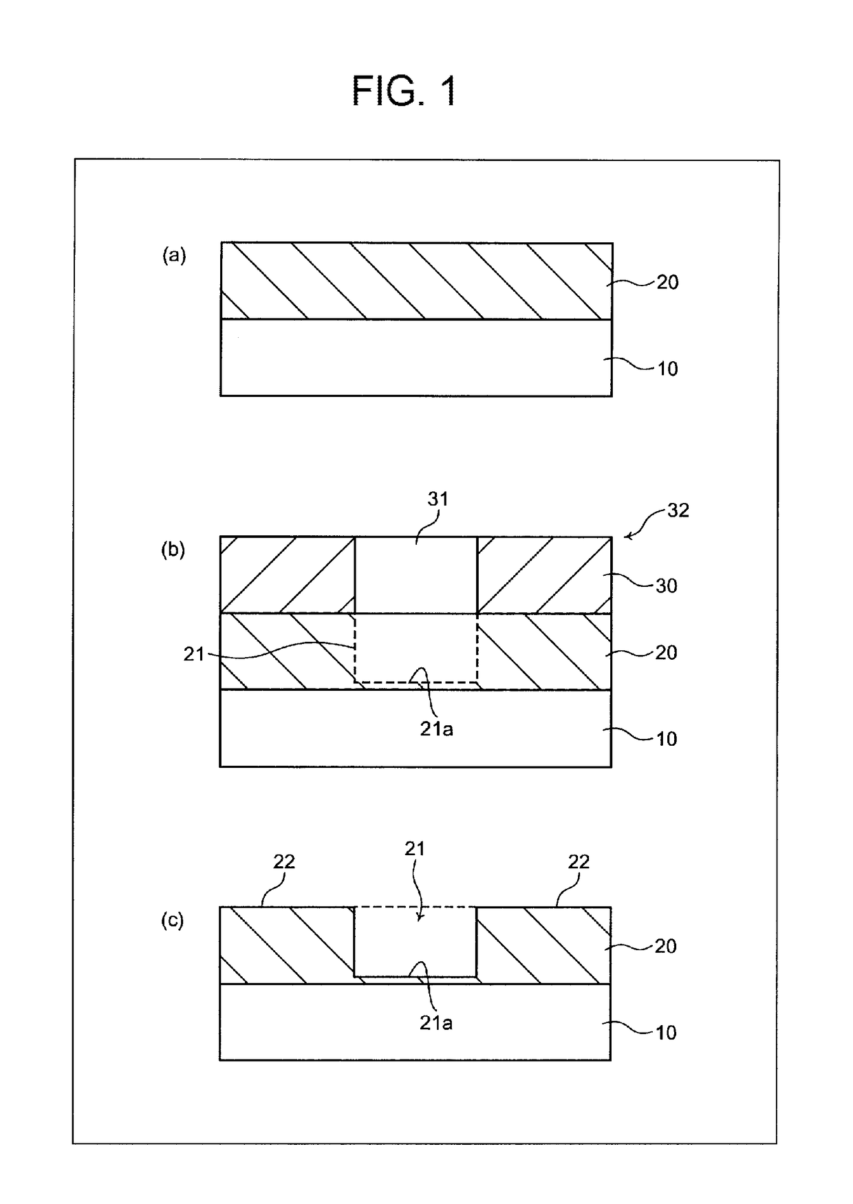
[0029]A method for manufacturing a silicon carbide semiconductor element according to Embodiment 1 of the invention will be described. FIG. 1 is a cross-sectional view illustrating a process of manufacturing the silicon carbide semiconductor element according to Embodiment 1 of the invention.

[0030]First, as illustrated in FIG. 1(a), for example, an n− silicon carbide single-crystal substrate (hereinafter, referred to as an n− silicon carbide substrate) 10 which is made of four-layer periodic hexagonal silicon carbide (4H—SiC) and in which an n− silicon carbide epitaxial layer is formed on one main surface of an n+ silicon carbide substrate is prepared.

[0031]Then, an inorganic insulating film 20 which functions as an ion implantation mask is deposited (formed) with a thickness of 1 μm on the main surface of the n− silicon carbide substrate 10. Then, as illustrated in FIG. 1(b), a photoresist 30 is applied onto the surface of the inorganic insulating film 20 and exposure and developme...

embodiment 2

[0049]Next, a method for manufacturing a silicon carbide semiconductor element according to Embodiment 2 will be described. FIG. 4 is a cross-sectional view illustrating the shape of an ion implantation mask according to Embodiment 2 of the invention. An inorganic insulating film 20 which functions as an ion implantation mask is deposited with a thickness of 1 μm on a main surface of an n− silicon carbide substrate 10, a photoresist 30 is applied onto the surface of the inorganic insulating film 20, and a resist pattern 32 is formed by the same processes as those in Embodiment 1. Then, dry etching is performed using the resist pattern 32 as a mask.

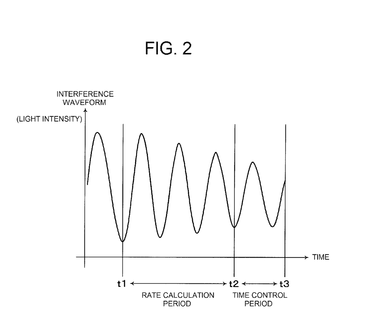
[0050]When the etching time is manually set, the initial thickness of a film, the thickness of a residual film, and the etching rate are calculated by the same method as that in Embodiment 1. When the thickness of the residual film is 400 nm and the etching rate is 60 nm per minute, etching is performed for 6.7 minutes to manufacture the i...

example

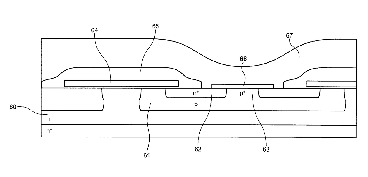
[0055]Next, the verification result of the surface shape of an opening portion 21 of a silicon carbide semiconductor element which is manufactured by the method for manufacturing the silicon carbide semiconductor element according to the embodiment of the invention will be described. FIG. 6 is a cross-sectional view illustrating a manufactured MOSFET.

[0056]First, a SiO2 film with a thickness of 1.5 μm was formed using an atmospheric pressure CVD apparatus on an n− silicon carbide substrate (the upper surface of an n− silicon carbide epitaxial layer 60), which was made of four-layer periodic hexagonal silicon carbide (4H—SiC) and in which the n− silicon carbide epitaxial layer 60 was formed on an n+ silicon carbide substrate. Then, an ion implantation mask 20 was formed on the n− silicon carbide substrate according to the embodiment and Al ions were implanted through the opening portion 21 to form a p region (p base layer) 61 in a surface layer of the n− silicon carbide substrate (a ...


PUM

PropertyMeasurementUnit
thicknessaaaaaaaaaa
temperatureaaaaaaaaaa
thicknessaaaaaaaaaa

Abstract

An ion implantation mask, which is an inorganic insulating film, is formed on a silicon carbide substrate. A mask portion and two regions of an opened ion implantation portion are formed in the ion implantation mask by dry etching. At that time, a residual portion which is thinner than the mask portion is formed in the bottom of the opened ion implantation portion. Then, ions are implanted through the ion implantation mask to form a predetermined semiconductor region in the silicon carbide substrate. According to this structure, it is possible to prevent an increase in the roughness of the surface of the silicon carbide substrate and to improve breakdown voltage.

Description

CROSS-REFERENCE TO RELATED APPLICATION(S)[0001]This non-provisional application for a U.S. Patent is a Continuation of International Application PCT / JP2014 / 065997 filed Jun. 17, 2014, which claims priority from JP PA 2013-131086 filed Jun. 21, 2013, the entire contents of both of which are hereby incorporated by reference.BACKGROUND OF THE INVENTION[0002]1. Field of the Invention[0003]The present invention relates to a method for manufacturing a silicon carbide semiconductor element using silicon carbide as a semiconductor material, and more particularly, to a silicon carbide semiconductor element in which a current flows from a front surface to a rear surface of a semiconductor substrate.[0004]2. Background of the Related Art[0005]Single-crystal silicon carbide (SiC) has a band gap or breakdown field strength that is significantly more than that of single-crystal silicon (Si). On-resistance which is resistance in an on state is inversely proportional to the cube of the breakdown fi...

Claims


Application Information

Patent Timeline
Patent Type & Authority Patents(United States)
IPC IPC(8): H01L21/04H01L21/66H01L21/311H01L29/16H01L29/12
CPCH01L21/0465H01L21/31116H01L22/12H01L22/26H01L29/12H01L29/1608H01L29/66068H01L29/7802
Inventor UTSUMI, MAKOTOSAKAI, YOSHIYUKI
Owner FUJI ELECTRIC CO LTD
Why Eureka
Try Eureka