Organic transistor and method for manufacturing same

a technology of organometallic transistors and manufacturing methods, which is applied in the direction of thermoelectric device junction materials, semiconductor devices, electrical apparatus, etc., can solve problems such as unsuitable improvement, achieve the effects of improving the regularity of crystals, facilitating the crystal growth of molecules, and increasing grain siz

Inactive Publication Date: 2014-10-09
TOKYO ELECTRON LTD
View PDF3 Cites 0 Cited by
  • Summary
  • Abstract
  • Description
  • Claims
  • Application Information

AI Technical Summary

Benefits of technology

[0019]As described above, the work of bonding the first insulating layer and the organic semiconductor layer is controlled to facilitate the crystal growth of molecules forming the organic semiconductor layer and further to increase a grain size. As a consequence, the regularity of crystal is improved, and the surface of the organic semiconductor layer can be planarized. As a result, it is possible to reduce a carrier mobility barrier in a channel area of the interface between the organic semiconductor layer and the second insulating layer and improve the mobility of the organic transistor.

Problems solved by technology

However, the proposals of Patent Documents 1 to 3 are designed for the organic transistor having a bottom gate type structure and thus are not suitable for the improvement of the mobility of the organic transistor having a top gate type structure in which a channel is formed by laminating a gate insulating layer on an organic semiconductor layer.

Method used


Image

  • Organic transistor and method for manufacturing same
  • Organic transistor and method for manufacturing same
  • Organic transistor and method for manufacturing same

Examples


first embodiment

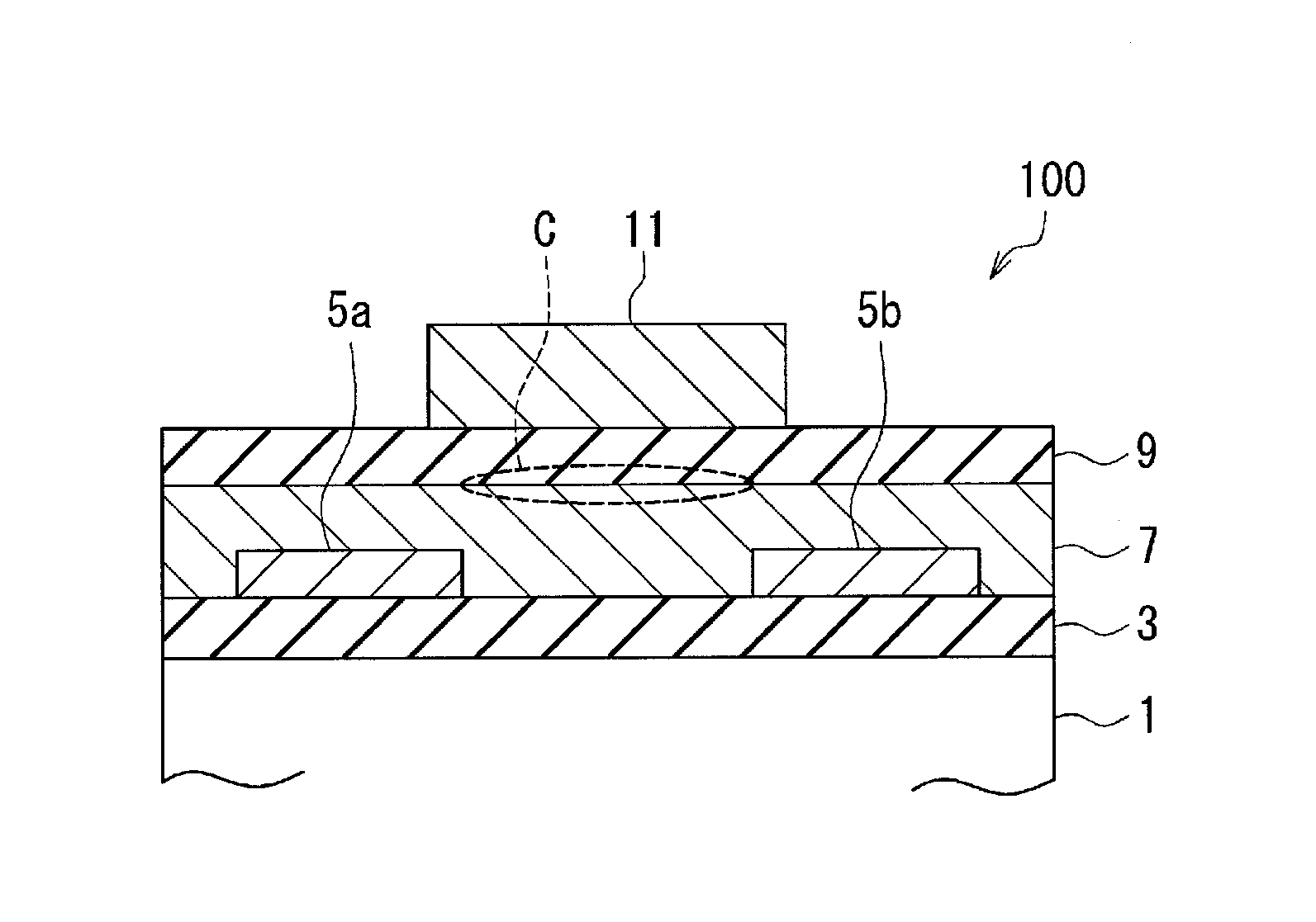
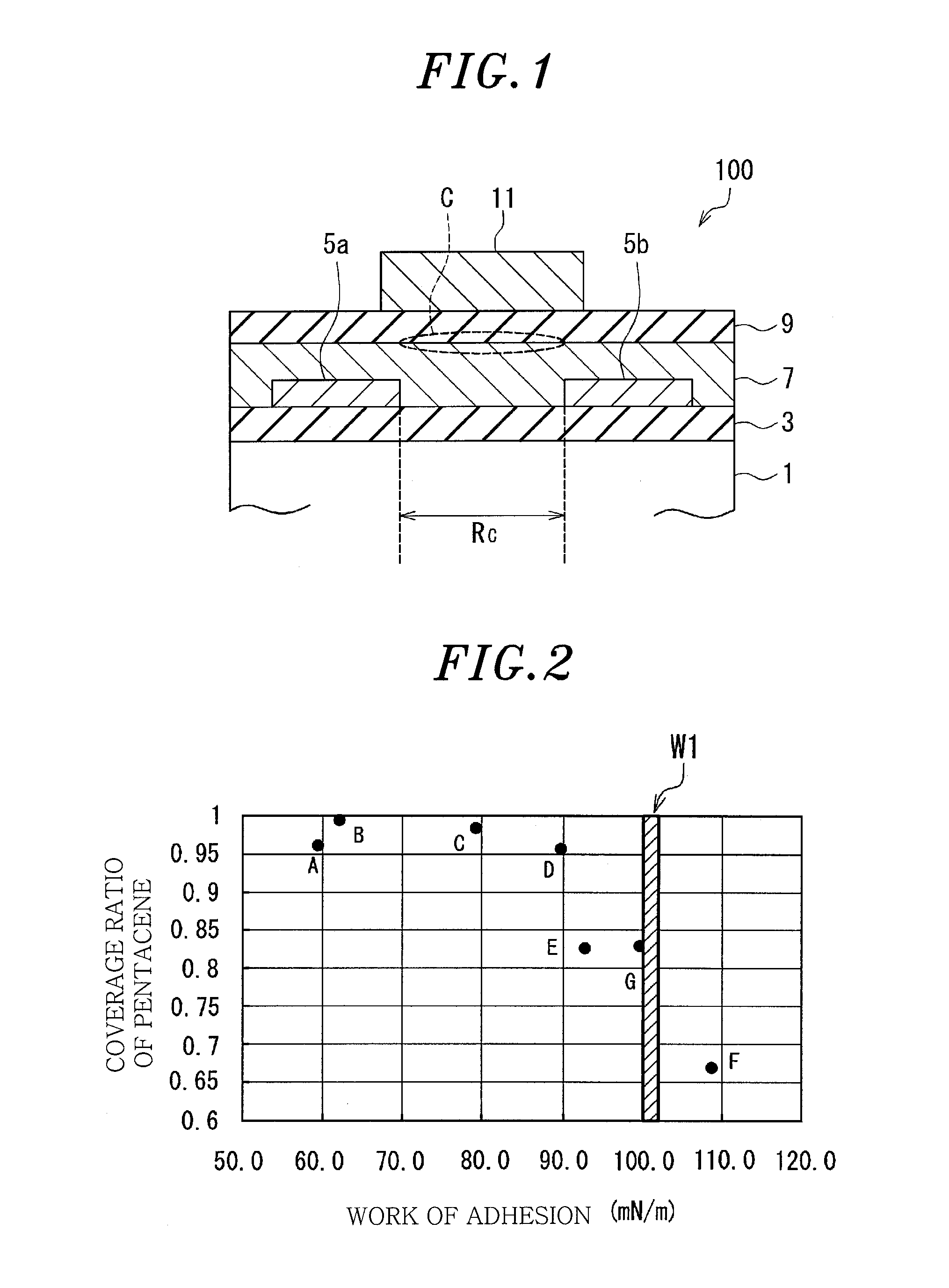
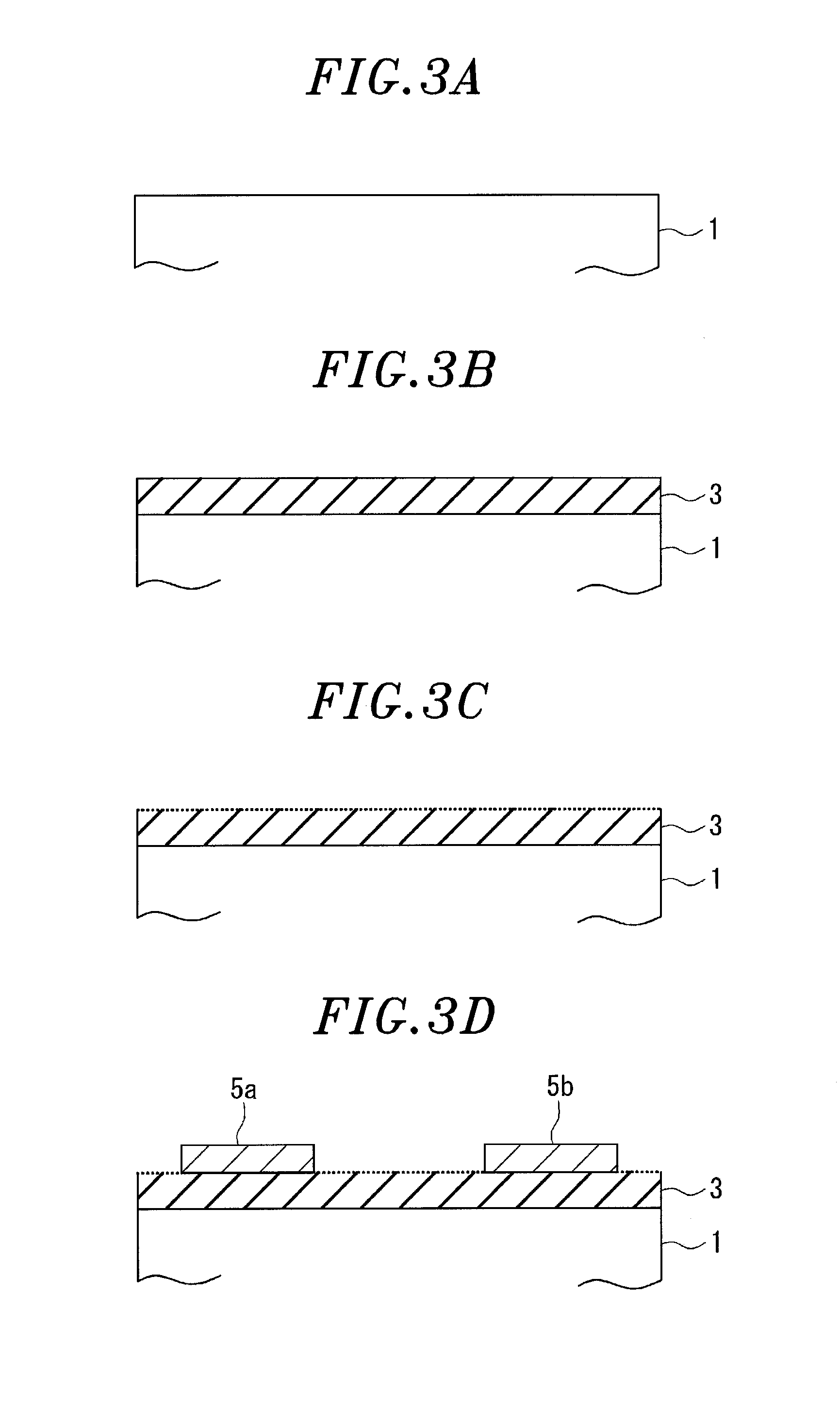
[0029]FIG. 1 is a cross sectional view showing a schematic configuration of an organic transistor 100 in accordance with a first embodiment of the present invention. The organic transistor 100 has a so-called top gate / bottom contact type structure. In other words, the organic transistor 100 includes: a substrate 1 that is a supporting body; a base insulating layer 3 that is a first insulating film formed on the substrate 1 with a predetermined thickness; a pair of source / drain electrodes 5a and 5b formed in a predetermined pattern on a part of the base insulating layer 3; an organic semiconductor layer 7 laminated so as to cover the source / drain electrodes 5a and 5b and be in contact with the base insulating layer 3; a gate insulating layer 9 as a second insulating layer laminated on the organic semiconductor layer 7; and a gate electrode 11 laminated on the gate insulating layer 9. The surface treatment is performed on the surface of the base insulating layer 3 which is in contact ...

second embodiment

[0094]Hereinafter, a second embodiment of the present invention will be described with reference to FIG. 7. FIG. 7 is a view for explaining a schematic configuration of an organic transistor in accordance with a second embodiment of the present invention. This organic transistor 101 has a so-called top gate / top contact structure. In other words, the organic transistor 101 includes: a substrate 1 that is a supporting body; a base insulating layer 3 that is a first insulating layer formed on the substrate 1 with a predetermined thickness; an organic semiconductor layer 7 laminated to be in contact with the base insulating layer 3; a pair of source / drain electrodes 5a and 5b formed on a part of the organic semiconductor layer 7 in a predetermined pattern; a gate insulating layer 9 that is a second insulating layer laminated on the organic semiconductor layer 7 between the source electrode 5a and the drain electrode 5b; and a gate electrode 11 laminated on the gate insulating layer 9. T...

third embodiment

[0098]Hereinafter, a method for manufacturing an organic transistor (not shown) in accordance with a third embodiment of the present invention will be described with reference to FIG. 8. In the first and the second embodiment, the surface treatment step is performed by the first treatment (i) for inactivating the surface of the base insulating layer 3, the second treatment (ii) for reducing active species on the surface of the base insulating layer 3, or the third treatment (iii) for removing moisture from the surface of the base insulating layer 3, as described above. In the present embodiment, a cleaning treatment for cleaning the surface of the base insulating layer 3 is performed as the surface treatment step before the treatment such as the first treatment (i), the second treatment (ii) or the third treatment (iii) is performed. In other words, in the present embodiment, the surface treatment step includes the treatment such as the first treatment (i), the second treatment (ii)...


PUM


Abstract

A method for manufacturing an organic transistor includes laminating a base insulating layer on a substrate; forming source/drain electrodes on the base insulating layer; laminating an organic semiconductor layer to cover the electrodes and be in contact with the base insulating layer; laminating a gate insulating layer on the organic semiconductor layer; forming a gate electrode on the gate insulating layer; and performing, before the organic semiconductor layer is formed, surface treatment on the surface of the base insulating layer which is in contact with the organic semiconductor layer. The surface treatment is performed such that, when W1 represents the work of adhesion between two laminated layers using the same material of the organic semiconductor layer, the work of adhesion W2 between the base insulating layer and the organic semiconductor layer when the organic semiconductor layer is formed on the surface-treated base insulating layer satisfies the relationship W1≧W2.

Description

FIELD OF THE INVENTION[0001]The present invention relates to an organic transistor and a method for manufacturing the same.BACKGROUND OF THE INVENTION[0002]An organic transistor is a transistor using an organic semiconductor material. Currently, the organic transistor has a field effect mobility (hereinafter, simply referred to as “mobility”) of about 1 cm2 / Vsec which is equal to that of amorphous silicon. The organic transistor is mainly classified into a top gate type structure and a bottom gate type structure in accordance with arrangement of a gate electrode. In the case of the top gate type structure, a channel is formed by laminating a gate insulating layer on an organic semiconductor layer. It is considered that the organic semiconductor layer is preferably made of a crystallized organic semiconductor material due to a high mobility.[0003]Currently, the organic semiconductor layer is formed by deposition or coating. In that case, however, the organic semiconductor material be...

Claims


Application Information

Patent Timeline
Patent Type & Authority Applications(United States)
IPC IPC(8): H01L51/05H01L51/00
CPCH01L51/0541H01L51/0002H01L51/0558H10K10/464H10K10/484H10K71/10
Inventor FUSE, TAKASHISAITO, MISAKOSATO, HIROSHI
Owner TOKYO ELECTRON LTD
Why Eureka
Try Eureka