

JFET structure for integrated circuit and fabrication method
a semiconductor and integrated circuit technology, applied in the field of semiconductor integrated circuits, can solve the problems of power consumption and much higher cost than a standard cmos process, and achieve the effects of reducing the amount of charge, and improving noise performan
- Summary
- Abstract
- Description
- Claims
- Application Information
AI Technical Summary
Benefits of technology
Problems solved by technology
Method used
Image

Examples
Embodiment Construction
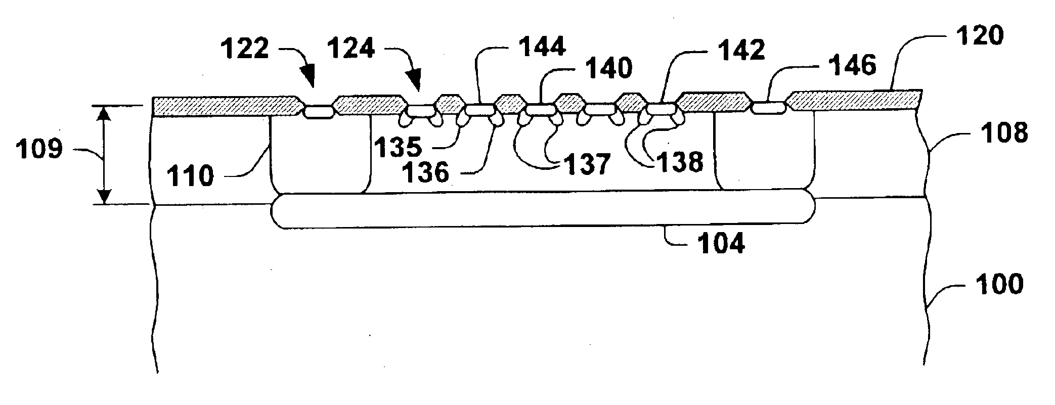
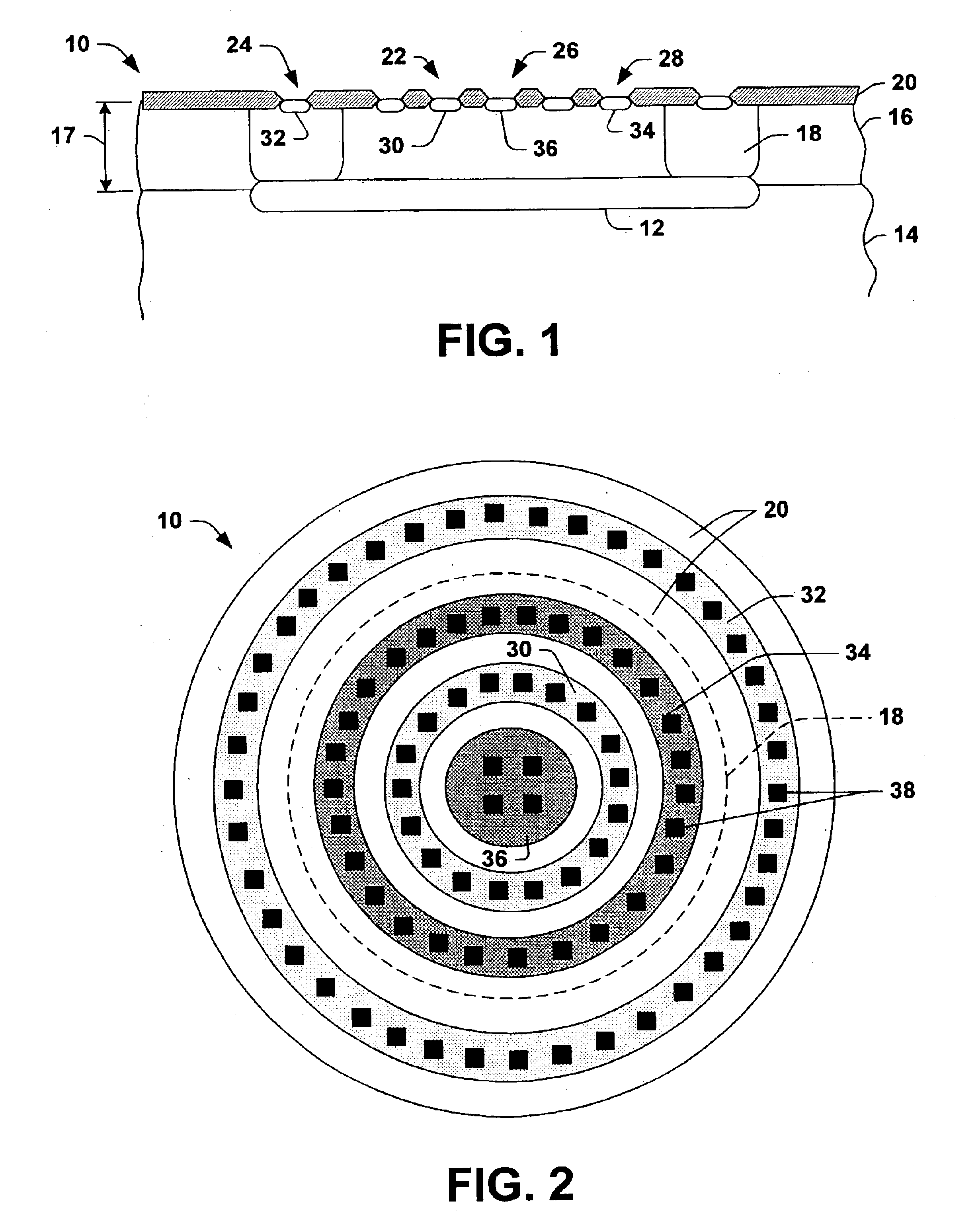
The present invention relates generally to junction field effect transistors (JFETs) and to fabrication methods for JFETs. For example, the JFET can be fabricated with an epitaxial layer that forms a sufficiently thick channel region to enable the JFET for use in high voltage applications (e.g., having a breakdown voltage greater than about 20V). Noise performance can be improved by employing threshold voltage (VT) implants at one or more of the gate, source and drain regions. Additionally, fabrication of a JFET can be facilitated by implementing all parts concurrently with a CMOS fabrication process and / or with a Bi-CMOS fabrication process. Another aspect of the present invention provides a three-terminal JFET structure, which can be fabricated individually or concurrently with a CMOS fabrication process and / or with a Bi-CMOS fabrication process.
FIGS. 1 and 2 illustrate a JFET 10 that can be fabricated in accordance with an aspect of the present invention. In this example, the JFE...
PUM
 Abstract
Description
Claims
Application Information