Electrical circuit apparatus and methods for assembling same

a technology of electrical circuit boards and circuit boards, applied in the direction of printed circuits, printed circuit aspects, stress/warp reduction of printed circuits, etc., can solve the problem of thermal expansion mismatch between load resistors, local distortion or warping of circuit boards after assembly, and the reliability of solder joints can also be significantly degraded

Active Publication Date: 2005-03-01
MOTOROLA SOLUTIONS INC
View PDF2 Cites 21 Cited by
  • Summary
  • Abstract
  • Description
  • Claims
  • Application Information

AI Technical Summary

Problems solved by technology

Moreover, load resistors are typically made of a ceramic material, which presents a thermal expansion mismatch between the load resistor and the heat sink since the heat sink typically has a higher coefficient of thermal expansion (CTE) than the ceramic load resistor.
This CTE mismatch can result in local distortion or warping of the circuit board after assembly.
Solder joint reliability can also be significantly degraded in a thermal cycling application.
Due to the fragility of the substrate, large fixtures are usually required for its alignment and protection during processing.
The use of fixtures usually forces manual processing.
One disadvantage of the hybrid manufacturing process is that it is more costly than other manufacturing methods primarily due to the added cost of the fixtures used in the process and also due to the need for a number of manual steps that generate a lower production throughput.
An additional disadvantage is that manufacturing with fixtures produces a significant variation in part placement and solder attachment due to fixture tolerances or due to fixture degradation with repeated use.
A primary disadvantage of the two pass reflow process is that it requires one high-temperature reflow pass with a high melting temperature solder alloy, and a second subsequent reflow pass with a lower melting temperature solder allow.
The first pass exposes the circuit board to high temperature, which can result in damage such as distortion.
The requirement of two independent passes with different solder temperature settings limits manufacturing throughput.
The two pass approach also does not lend itself well to no-lead solder because the first temperature needed to attach the heat sinks would have to exceed the elevated no-lead solder reflow temperature.
This is a significant disadvantage because no-lead solder attachment may likely become a key product differentiator in the near future since some markets, especially European markets, are moving toward requiring no-lead solder attachment.
In addition, neither the hybrid manufacturing process nor the two pass solder reflow process addresses the thermal expansion mismatch issues that arise when mounting devices such as ceramic load resistors to a circuit board.

Method used


Image

  • Electrical circuit apparatus and methods for assembling same
  • Electrical circuit apparatus and methods for assembling same
  • Electrical circuit apparatus and methods for assembling same

Examples


Embodiment Construction

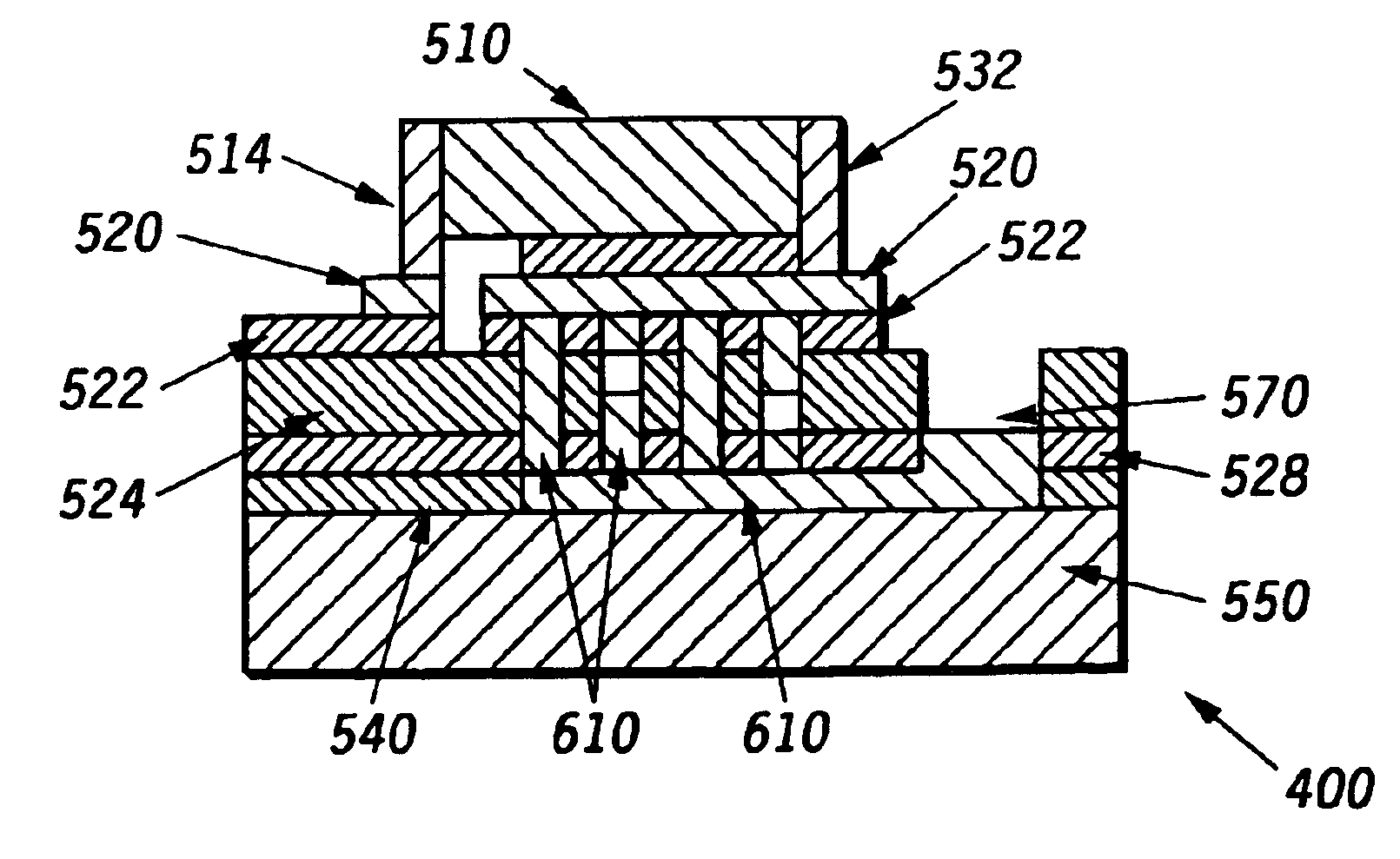
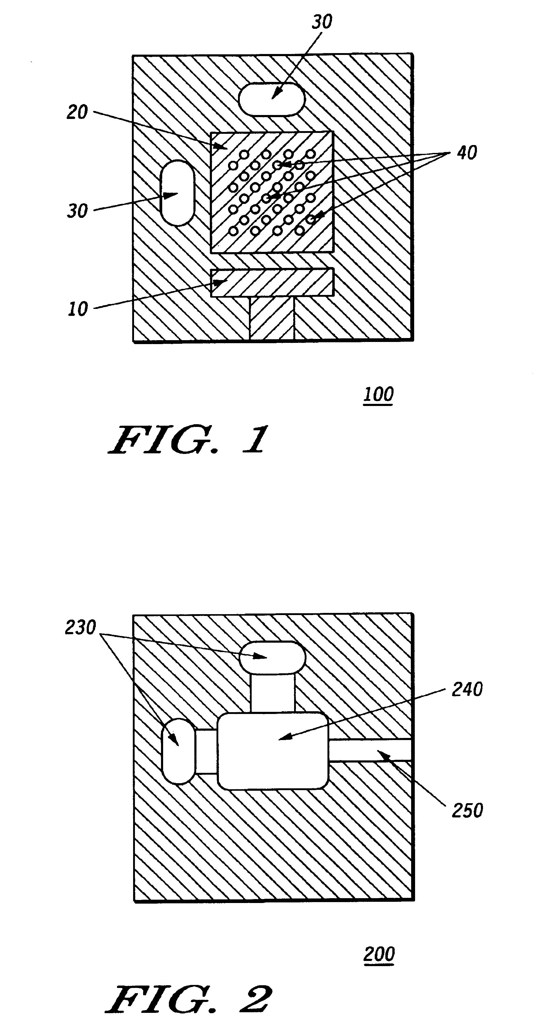
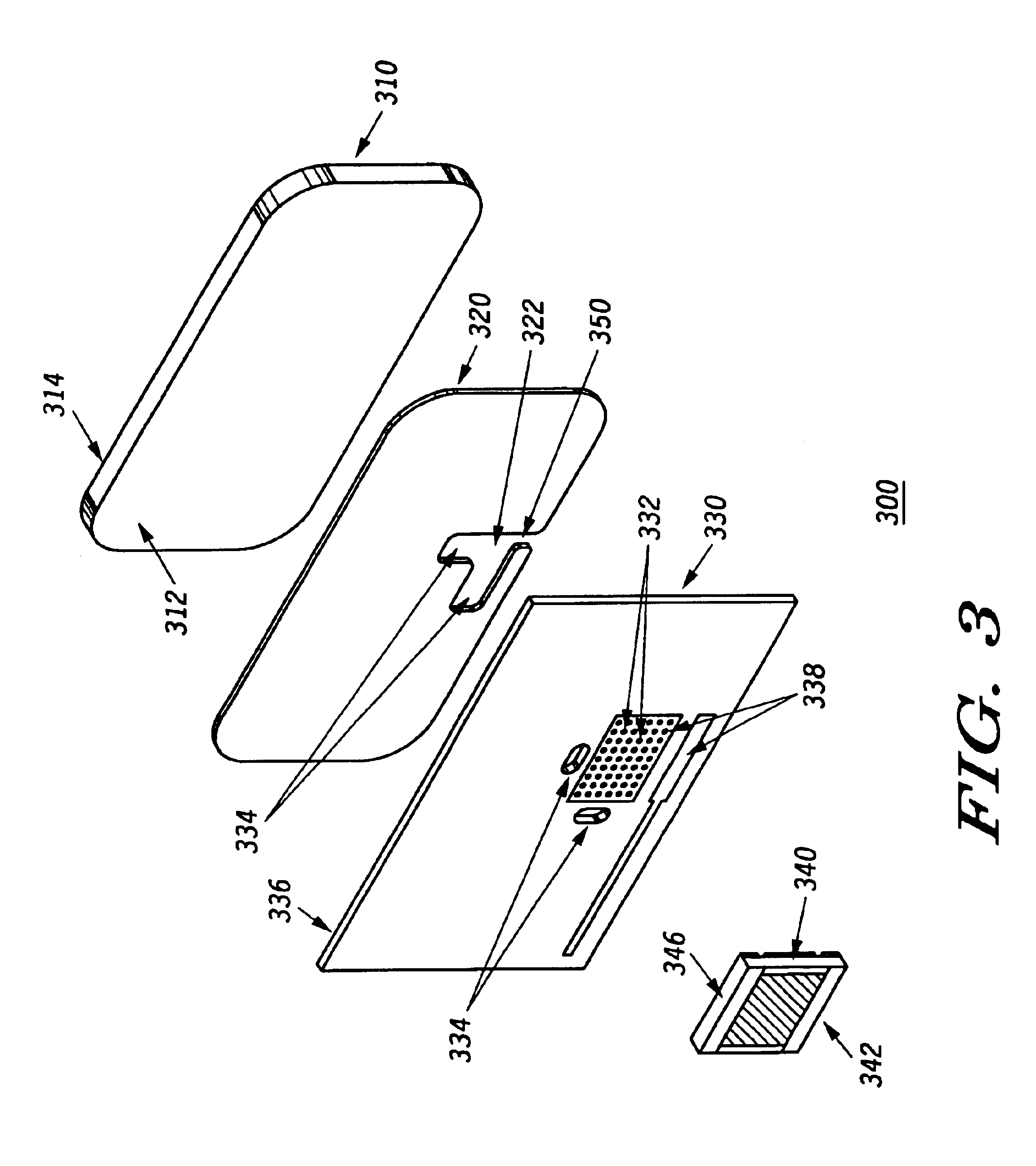
While this invention is susceptible of embodiments in many different forms, there are shown in the figures and will herein be described in detail specific embodiments, with the understanding that the present disclosure is to be considered as an example of the principles of the invention and not intended to limit the invention to the specific embodiments shown and described. Further, the terms and words used herein are not to be considered limiting, but rather merely descriptive. It will also be appreciated that for simplicity and clarity of illustration, elements shown in the figures have not necessarily been drawn to scale. For example, the dimensions of some of the elements are exaggerated relative to each other. Further, where considered appropriate, reference numerals have been repeated among the figures to indicate corresponding elements.

The present invention includes a method and electrical circuit apparatus, wherein components may be mounted to a circuit board. In a first asp...


PUM


Abstract

An electrical circuit apparatus (300) that includes: a substrate (330) having a ground layer (336), at least one thermal aperture (332), and at least one solder aperture (334); a heat sink (310); and an adhesive layer (320) for mechanically coupling the heat sink to the ground layer of the substrate such that at least a portion of the at least one substrate thermal aperture overlaps the heat sink, the adhesive layer having at least one thermal aperture (322) and at least one solder aperture (324), wherein aligning the at least one substrate solder aperture with the at least one adhesive layer solder aperture and aligning the at least one substrate thermal aperture with the at least one adhesive layer thermal aperture enables solder wetting in a predetermined area between the heat sink and the ground layer of the substrate.

Description

FIELD OF THE INVENTIONThe present invention relates generally to methods and electrical circuit apparatus, wherein components are mounted to a circuit board.BACKGROUND OF THE INVENTIONWhen constructing power amplifiers various components must be mounted to a circuit board or substrate. Many of these components are mounted to a top side of the circuit board using a known solder reflow process. For instance, a load resistor having at least one input terminal and having a ground portion or flange may be mounted to the top side of the circuit board. When mounting a load resistor to a circuit board, three factors must be balanced. First, the load resistor must have a proper and sufficient electrical connection to the circuit board, wherein the input terminals are soldered to the top side of the circuit board and the ground flange is sufficiently coupled to a heat sink that is typically soldered locally to the underside of the circuit board in an area primarily surrounding the load resist...

Claims


Application Information

Patent Timeline
Patent Type & Authority Patents(United States)
IPC IPC(8): H01L23/367H01L23/34H05K3/00H05K1/02H05K3/34H05K3/38H05K1/11H05K3/44
CPCH01L23/3677H05K1/0206H05K3/0061H05K1/0271H01L2924/0002H05K1/111H05K3/341H05K3/386H05K3/44H05K2201/0347H05K2201/068H05K2201/09063H05K2201/1003H05K2203/1178H01L2924/00
Inventor WALDVOGEL, JOHN M.BIELICK, BRIAN R.MILLER, HERMAN J.VAN CANNON, BILLY J.
Owner MOTOROLA SOLUTIONS INC
Why Eureka
Try Eureka