Amplitude converting circuit
- Summary
- Abstract
- Description
- Claims
- Application Information
AI Technical Summary
Benefits of technology
Problems solved by technology
Method used
Image
Examples
first embodiment
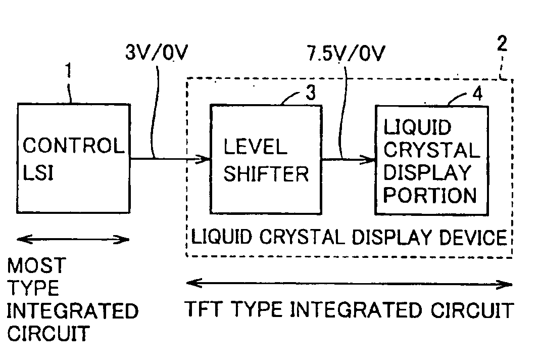
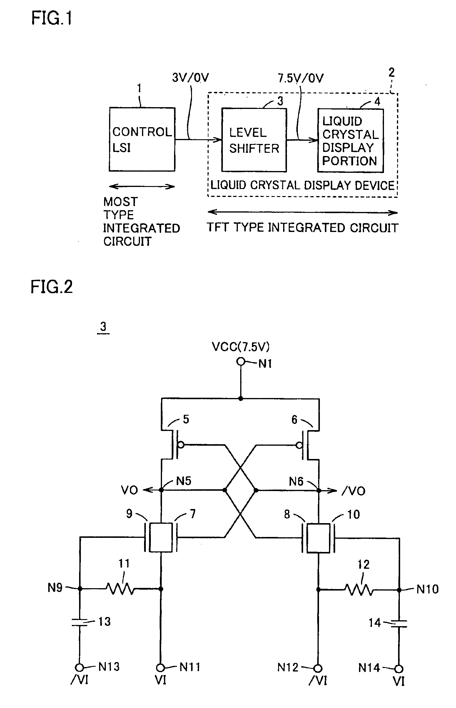
FIG. 1 is a block diagram representing a configuration of a portion related to image display of a portable telephone in accordance with a first embodiment of the present invention.
Referring to FIG. 1, the portable telephone includes a control LSI 1, which is an MOST type integrated circuit, and a liquid crystal display device 2, which is a TFT type integrated circuit, and liquid crystal display device 2 includes a level shifter 3 and a liquid crystal display portion 4.
Control LSI 1 outputs a control signal for liquid crystal display device 2. The “H” level of the control signal is 3V, and the “L” level is 0V. Though a number of control signals are generated actually, only one control signal will be described here for simplicity. Level shifter 3 converts logic level of the control signal from control LSI 1 and generates an internal control signal. The “H” level of this internal control signal is 7.5V and the “L” level is 0V. Liquid crystal display portion 4 displays images in accorda...
second embodiment
FIG. 9 is a circuit diagram representing a configuration of a level shifter 30 in accordance with a second embodiment of the present invention, comparable to FIG. 7. Referring to FIG. 9, level shifter 30 differs from level shifter 23 shown in FIG. 7 in that resistance elements 31, 32 and capacitors 33, 34 are added. Resistance element 31 is inserted between node N1 of the power supply potential VCC and the gate of N type TFT 21 (node N21), and resistance element 32 is inserted between node N1 and the gate of N type TFT 22 (node N22). Capacitor 33 is connected between nodes N11 and N21, and capacitor 34 is connected between nodes N 12 and N22.
FIG. 10 is a time chart representing an operation of level shifter 30. Referring to FIG. 10, in the initial state, input signals VI and VI are set to the “H” level (3V) and the “L” level (0V), respectively, and the output signals VO and / VO are set to the “H” level (7.5V) and the “L” level (0V), respectively. Nodes N21 and N22 are receiving the ...
third embodiment
FIG. 11 is a circuit diagram representing a configuration of a level shifter 35 in accordance with a third embodiment of the present invention, comparable to FIG. 9. Referring to FIG. 11, level shifter 35 differs from level shifter 30 shown in FIG. 9 in that N type TFTs 21 and 22 are replaced by P type TFTs 36 and 37. P type TFT 36 is connected between nodes N9 and N11, with its gate connected to node N21. P type TFT 37 is connected between nodes N10 and N12, with its gate connected to node N22.
Further, resistance element 31 is connected between node N21 and a node N31 of a negative power supply potential −VCC (−7.5V). Resistance element 32 is connected between node N22 and a node N32 of the negative power supply potential −VCC (−7.5V). Capacitor 33 is connected between nodes N13 and N21, and capacitor 34 is connected between nodes N14 and N22.
FIG. 12 is a time chart representing an operation of level shifter 35. Referring to FIG. 12, in the initial state, the input signals VI and / ...
PUM
 Abstract
Description
Claims
Application Information


