Semiconductor device which is low in power and high in speed and is highly integrated

a semiconductor device and high-speed technology, applied in semiconductor devices, digital storage, instruments, etc., can solve the problems of large current required for writing, phase change memory also has a large current, etc., and achieve low power at a write time, high integration, and small current consumption

Inactive Publication Date: 2005-03-01
HITACHI LTD
View PDF6 Cites 46 Cited by
  • Summary
  • Abstract
  • Description
  • Claims
  • Application Information

AI Technical Summary

Benefits of technology

An object of the present invention is to realize a high-speed nonvolatile memory which has a small current consumption and low power at a write time and which is highly integrated.
To achieve the above-described object, according to the present invention, there is provided one of representative means as follows. That is, there is provided a nonvolatile semiconductor memory in which a current is passed through a data line to write data in a memory cell. In the memory, the data is read from the selected memory cell during a write operation, and inverting / writing is performed only with respect to a bit which disagrees with input data inputted from the outside. More preferably, the memory includes: an encoder for encoding the data of a plurality of selected memory cells so as to reduce the number of data to be inverted and forming write data of the plurality of memory cells; and a decoder for decoding the data read from the plurality of selected memory cells and forming output data to be outputted to the outside.

Problems solved by technology

Furthermore, the phase change memory also has a large current required for the writing, because a sufficient temperature rise is caused in the phase change resistance.

Method used


Image

  • Semiconductor device which is low in power and high in speed and is highly integrated
  • Semiconductor device which is low in power and high in speed and is highly integrated
  • Semiconductor device which is low in power and high in speed and is highly integrated

Examples


first embodiment

(First Embodiment)

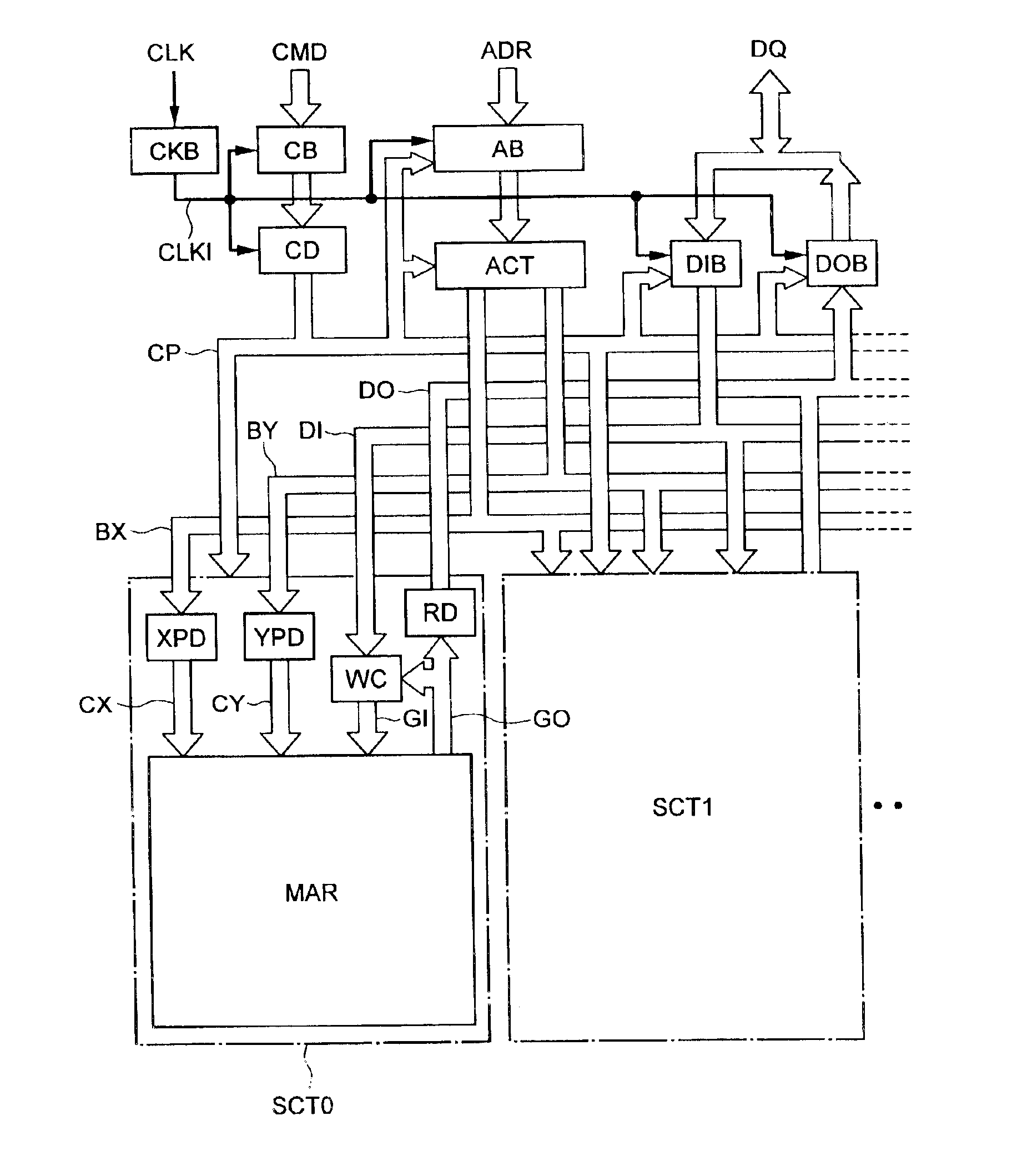
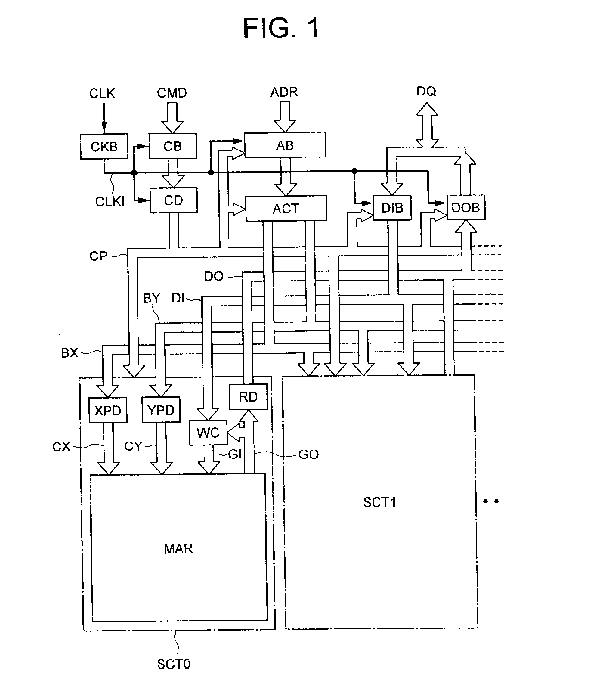
FIG. 1 is a main part block diagram of a memory according to the present invention. A first embodiment is characterized in that a data encoder WC and data decoder RD are disposed. Here, the constitution example of a synchronous memory is shown. The example includes a clock buffer CKB, command buffer CB, command decoder CD, address buffer AB, address counter ACT, input buffer DIB, and output buffer DOB. Furthermore, sectors SCT0, SCT1, . . . including memory arrays MAR are disposed. The sector is disposed for each bank, but the bank may include a plurality of sectors. The sector further includes a row pre-decoder XPD, column pre-decoder YPD, data encoder WC, and data decoder RD.

Each circuit block has the following function. The clock buffer CKB distributes an external clock CLK as an internal clock CLKI to the command decoder CD. The command decoder CD generates a control signal CP for controlling the address buffer AB, column address counter YCT, input buffer DIB, ...

second embodiment

(Second Embodiment)

The method of reducing the number of written bits as described in the first embodiment is effective not only for the MRAM but also for the phase change memory. The phase change memory to which the present invention is applied can be constituted in the same manner as in the MRAM in FIG. 1, and data encoder and decoder shown in FIGS. 2 to 7 can be used. FIG. 17 shows the constitution example of the memory array. The constitution is used as the memory array MAR in FIG. 1. The constitution includes a memory cell array OCA, row decoder XDEC, word driver group WD, and data line control circuit CCO. Here, in the same manner as in FIG. 8, for the sake of simplicity, a dummy cell for generating a reference signal is omitted. Moreover, this constitution may be repeated to form the memory array MAR of FIG. 1 depending on the memory capacity. The memory cell array OCA includes memory cells OC disposed in the intersections of word lines WL0, WL1, WL2, WL3, . . . with data line...

third embodiment

(Third Embodiment)

Next, an embodiment in which the coding is not used will be described with respect to the MRAM. FIG. 21 shows another constitution example of the memory array of the MRAM. For example, the whole MRAM is constituted by removing the data encoder WC and data decoder RD from FIG. 1. This memory array constitution includes the memory cell array MCA, row decoder XDEC, word driver group WDP, and data line control circuits CCN2, CCF2. The memory cell array MCA is constituted as shown in FIG. 8, although the number of data lines differs. The row decoder XDEC and word driver group WDP operate in the same manner as in FIG. 8.

The data line control circuit CCN2 includes a column selector YSN, and a plurality of read / write circuits RWN for the read data GO0, GO1, . . . Here, for the sake of simplicity, the column decoders are omitted. The column selector YSN is constituted in the same manner as in the column selector YSN3 in FIG. 9, and connects the desired data line to the comm...


PUM


Abstract

There is disclosed a write operation of a MRAM in which a current necessary for inverting magnetization of an MTJ element has to be passed through a data line and therefore current consumption is large. The write operation comprises: comparing input data DI with read data GO read from a memory cell array and encoding the input data DI to form write data GI by a data encoder WC; and decoding the read data GO by a data decoder RD to form output data DO. In a nonvolatile semiconductor memory in which the current is passed through the data line to write data into a memory cell, the number of bits to be written during the write operation is reduced, and the current consumption can be reduced. This can realize the MRAM including a low-power highly-integrated memory.

Description

BACKGROUND OF THE INVENTION1. Field of the InventionThe present invention relates to a semiconductor device, particularly to a semiconductor device including a nonvolatile memory which uses a memory cell for storing information using a magnetic resistance or phase change resistance and which is low in power and high in speed and is highly integrated.2. Description of the Related ArtA magnetoresistive random access memory (MRAM) has been developed which is a nonvolatile memory but which has no limitation in the number of read / write operations. The MRAM stores information using a magnetoresistive effect in which a resistance of an element differs with a magnetization direction of a ferromagnetic material in a memory cell. In recent years, development of a magnetic tunnel junction (MTJ) element whose magnetoresistive change ratio referred to as magnetoresistance (MR) is larger than that of a related-art element, and application of the element to the MRAM have been advanced. It has been...

Claims


Application Information

Patent Timeline
Patent Type & Authority Patents(United States)
IPC IPC(8): G11C7/10G11C13/00G11C11/15H01L21/8246H01L27/10H01L27/105H01L43/08
CPCG11C7/1006G11C7/1078G11C11/1675G11C11/1673G11C7/1096
Inventor SAKATA, TAKESHIMATSUOKA, HIDEYUKI
Owner HITACHI LTD
Why Eureka
Try Eureka