Semiconductor device fabrication chamber cleaning method and apparatus with recirculation of cleaning gas

a technology of semiconductor devices and cleaning gas, which is applied in the field of semiconductor device processing, can solve the problems of contaminating the sensitive devices being processed in the chamber, and the conventional consumption of cleaning gas in the chamber cleaning process, so as to reduce the overall cost, both economic and environmental

Inactive Publication Date: 2005-03-08
APPLIED MATERIALS INC
View PDF40 Cites 451 Cited by
  • Summary
  • Abstract
  • Description
  • Claims
  • Application Information

AI Technical Summary

Benefits of technology

Methods and apparatus provided in accordance with the present invention allow a gas which flows from a processing chamber (an outlet gas) during a cleaning operation to be recirculated by separating out reaction products from the outlet gas. Because the outlet gas is recirculated and useful species are reused for cleaning, the total consumption of cleaning gas and the amount of undesirable emissions are reduced. Accordingly, the present invention may reduce the overall cost, both economic and environmental, of semiconductor device manufacturing.

Problems solved by technology

The accumulated material can crumble from chamber surfaces and cause contamination of the sensitive devices being processed in the chamber.
Unfortunately, such chamber cleaning processes conventionally consume considerable quantities of cleaning gases, and also produce undesirable by-products such as hazardous air pollutants (HAPs) and perfluorocompounds (PFCs), which are greenhouse gases that may contribute to global warming.

Method used


Image

  • Semiconductor device fabrication chamber cleaning method and apparatus with recirculation of cleaning gas
  • Semiconductor device fabrication chamber cleaning method and apparatus with recirculation of cleaning gas
  • Semiconductor device fabrication chamber cleaning method and apparatus with recirculation of cleaning gas

Examples


first embodiment

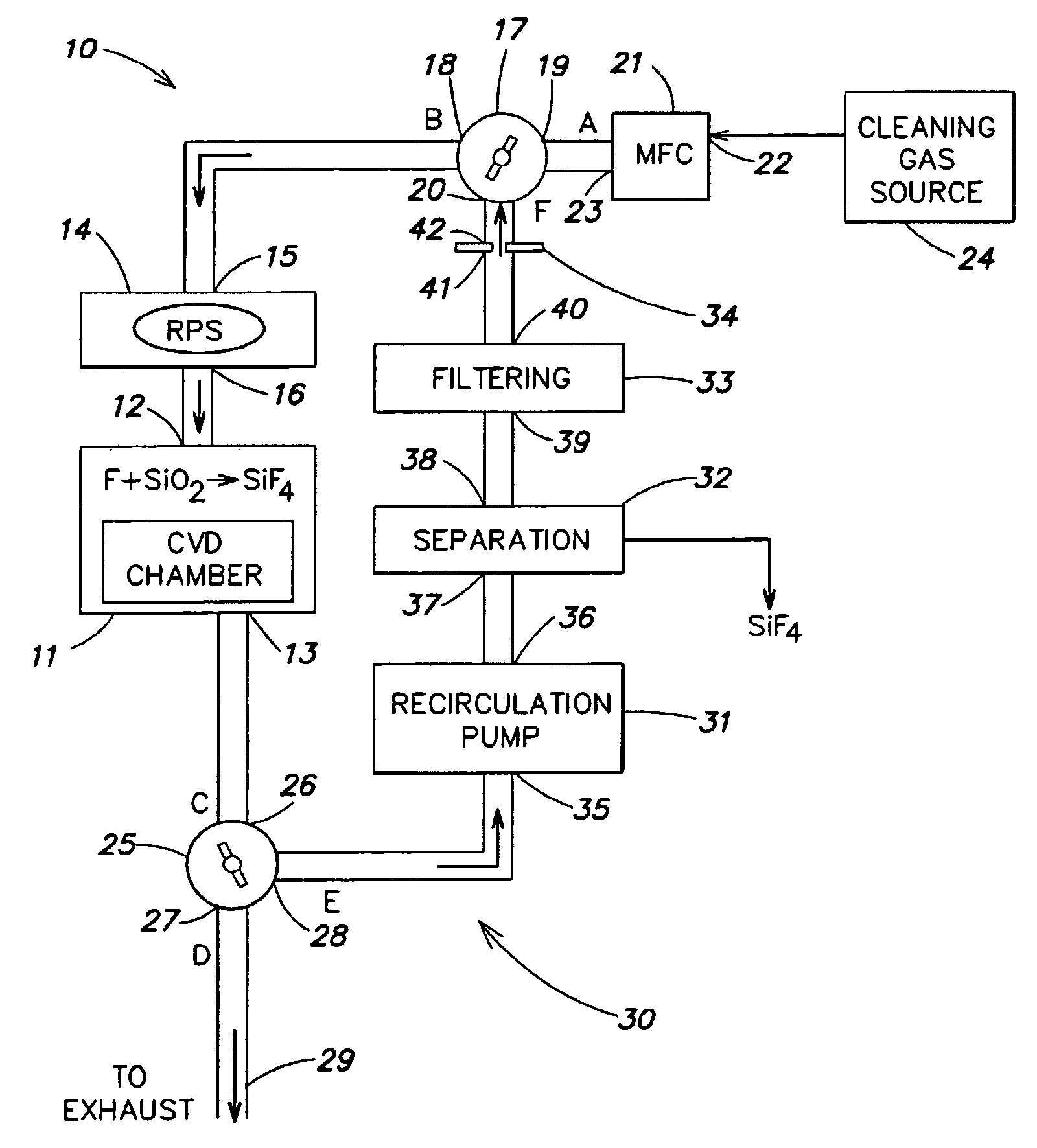
FIG. 1 is a schematic block diagram of a cleaning system 10 provided in accordance with a first embodiment of the invention. The cleaning system 10 includes a processing chamber 11 which is to be cleaned by the system 10. The processing chamber 11 includes an inlet 12 and an outlet 13. The processing chamber 11 may be any one of a number of different types of processing chambers used to perform various processes for fabrication of semiconductor devices. For example, the processing chamber 11 may be of a type used to carry out chemical vapor deposition or other types of semiconductor device fabrication processes. For example, the processing chamber 11 may be a deposition chamber such as an xZ style chamber available from Applied Materials, Inc., the assignee of this application or the Ultima high density plasma chemical vapor deposition (HDPCVD) chamber, also available from Applied Materials, Inc. Alternatively, the processing chamber 11 may be an etching chamber such as the eMax or ...

second embodiment

FIG. 3 is a diagramatic side view showing a second embodiment of the inventive cleaning system.

Referring to FIG. 3, reference numeral 211 generally indicates a substrate processing system. The processing system 211 includes a processing chamber 213 coupled to a source of precursor gas 214 (e.g., a source of NF3) via a remote plasma source 215 and coupled to a pump 217 (e.g., a mechanical pump, a turbo-molecular pump, etc.). Pump 217 is coupled to a main exhaust 219 (e.g., an exhaust used by a plurality of processing chambers such as a main exhaust of a clean room), and a recirculation line 221 is coupled between the pump 217 and the remote plasma source 215. The pump 217 is positioned adjacent the deposition chamber 213 to reduce recombination of at least one reactive species (e.g., F) when the reactive species travels from the processing chamber 213 to the pump 217, and the recirculation line 221 is also configured so as to have a relatively short length (e.g., to reduce recombinat...

third embodiment

FIG. 4 is a schematic block diagram that illustrates a cleaning system 400 provided in accordance with a third embodiment of the invention. Elements that this embodiment shares with the embodiment of FIG. 1 are labeled with the same reference numerals as in FIG. 1.

The system 400 includes a processing chamber 11. Upstream from the processing chamber 11 are a remote plasma source 14, a mass flow controller 21, a valve 401 and a cleaning gas source 24. Downstream from the processing chamber 11 is an exhaust pump 402. A conduit 404 connecting an outlet of the processing chamber 11 with the exhaust pump 402 is controlled by a throttle valve 406.

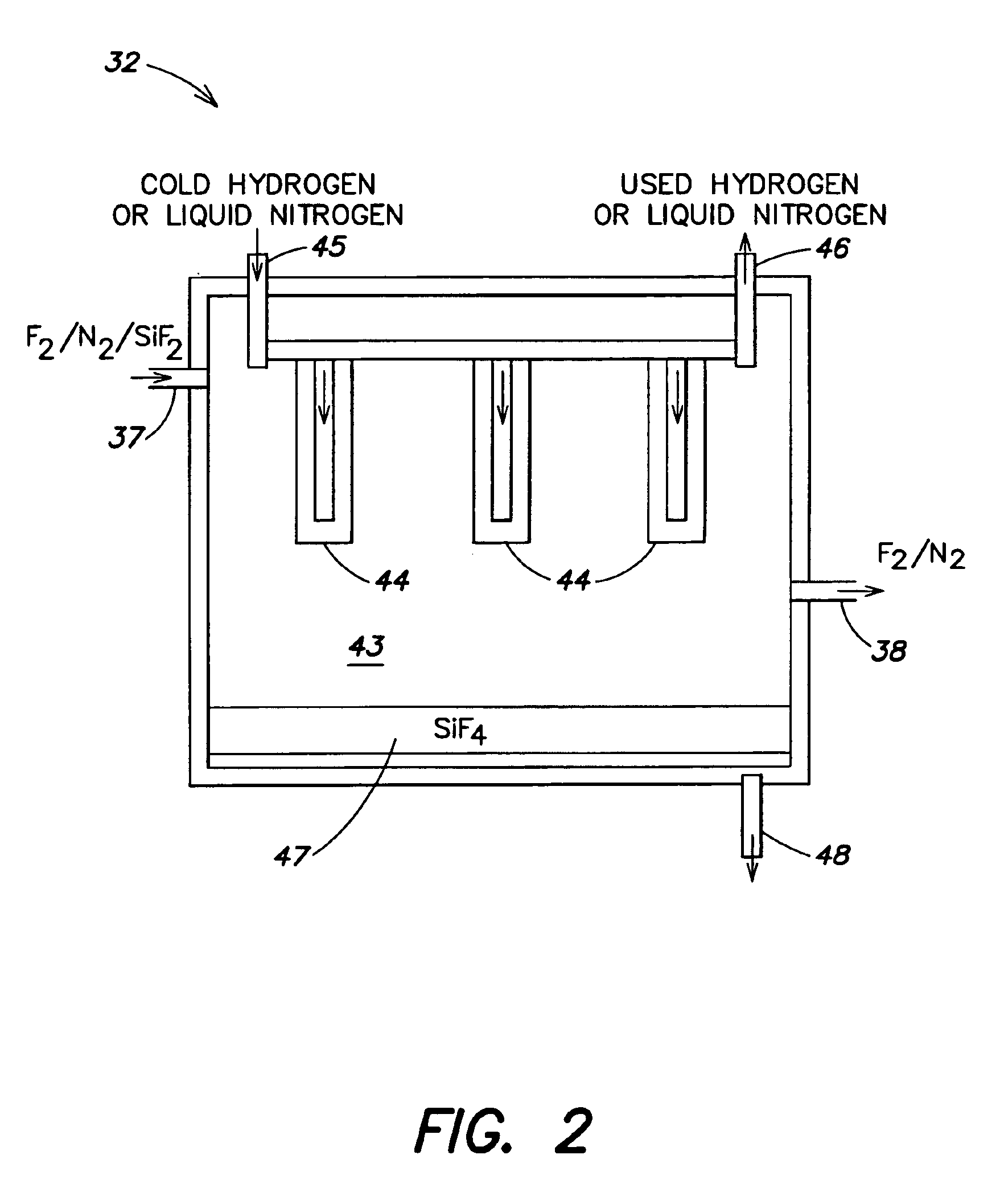
Branching off from conduit 404 is a recirculation path 408. The recirculation path 408 includes a valve 410, recirculation pump 31, a valve 414, an adsorption canister 416, a mass flow controller (MFC) 412, and a valve 418. A pressure interlock 422 is installed in the recirculation path 408 between the recirculation pump 31 and the MFC 412.

A desor...


PUM

PropertyMeasurementUnit
pressureaaaaaaaaaa
pressureaaaaaaaaaa
pressureaaaaaaaaaa

Abstract

A method of cleaning a semiconductor fabrication processing chamber involves recirculation of cleaning gas components. Consequently, input cleaning gas is utilized efficiently, and undesirable emissions are reduced. The method includes flowing a cleaning gas to an inlet of a processing chamber, and exposing surfaces of the processing chamber to the cleaning gas to clean the surfaces, thereby producing a reaction product. The method further includes removing an outlet gas including the reaction product from an outlet of the processing chamber, separating at least a portion of the reaction product from the outlet gas, and recirculating a portion of the outlet gas to the inlet of the processing chamber.

Description

FIELD OF THE INVENTIONThe present invention relates generally to semiconductor device processing, and is more specifically concerned with methods and apparatus for cleaning processing chambers employed in the fabrication of semiconductor devices.BACKGROUND OF THE INVENTIONManufacture of semiconductor devices such as liquid crystal displays, flat panel displays, and thin film transistors involves use of processing chambers in which various processes are carried out. Many of these processes can result in accumulation of material on chamber surfaces as a by-product of processes in which material is deposited on a substrate in layers (as by chemical vapor deposition (CVD), physical vapor deposition (PVD), thermal evaporation, etc.), or in which material is etched from substrate surfaces. The accumulated material can crumble from chamber surfaces and cause contamination of the sensitive devices being processed in the chamber. Accordingly, processing chambers must be cleaned of accumulate...

Claims


Application Information

Patent Timeline
Patent Type & Authority Patents(United States)
IPC IPC(8): B08B7/00C23C16/448C23C16/44C23C16/452H01J37/32C23C16/455
CPCB08B7/00B08B7/0035C23C16/4405C23C16/452H01J37/3244H01J37/32844C23C16/45593Y02C20/30H01J2237/335
Inventor SHAMOUILIAN, SHAMOUILLAI, CANFENGCOX, MICHAEL SANTIAGOKRISHNARAJ, PADMANABHANTANAKA, TSUTOMURAOUX, SEBASTIENPORSHNEV, PETER I.NOWAK, THOMAS
Owner APPLIED MATERIALS INC
Why Eureka
Try Eureka