Method and apparatus for parallel optical transceiver module assembly

a technology of parallel optical transceiver and module, applied in the field of network communication, can solve the problems of affecting the majority of failures of the transmitter and receiver module, and the sensitiveness/sensitivity of the optoelectronic device, etc., and achieve the effect of improving the yield of the modul

Inactive Publication Date: 2005-03-08
SUMITOMO ELECTRIC DEVICE INNOVATIONS U S A
View PDF246 Cites 23 Cited by
  • Summary
  • Abstract
  • Description
  • Claims
  • Application Information

AI Technical Summary

Benefits of technology

In view of the above-stated disadvantages of the prior art, an object of the present invention is to provide a modular processing method to manufacture parallel optical transmitter, receiver and / or transceiver modules to improve the yield of the modules in the manufacture process.

Problems solved by technology

Optoelectronic devices are sensitive and / or susceptible to temperature, humidity, and other environmental hazards due to the complexity and fabrication limits of these devices, which contribute to majority of the failure in the transmitter and receiver modules.
This causes the difficulty of rework, very high material cost if the part fails, and lack of effective in-line process diagnostic techniques during manufacture.
Moreover, the burn-in process, which stabilizes the array device performance and screens out “infant failures,” is usually conducted at the module level, which requires more complex test setup and longer burn-in time, and further increases the manufacturing cost.

Method used


Image

  • Method and apparatus for parallel optical transceiver module assembly
  • Method and apparatus for parallel optical transceiver module assembly
  • Method and apparatus for parallel optical transceiver module assembly

Examples


Embodiment Construction

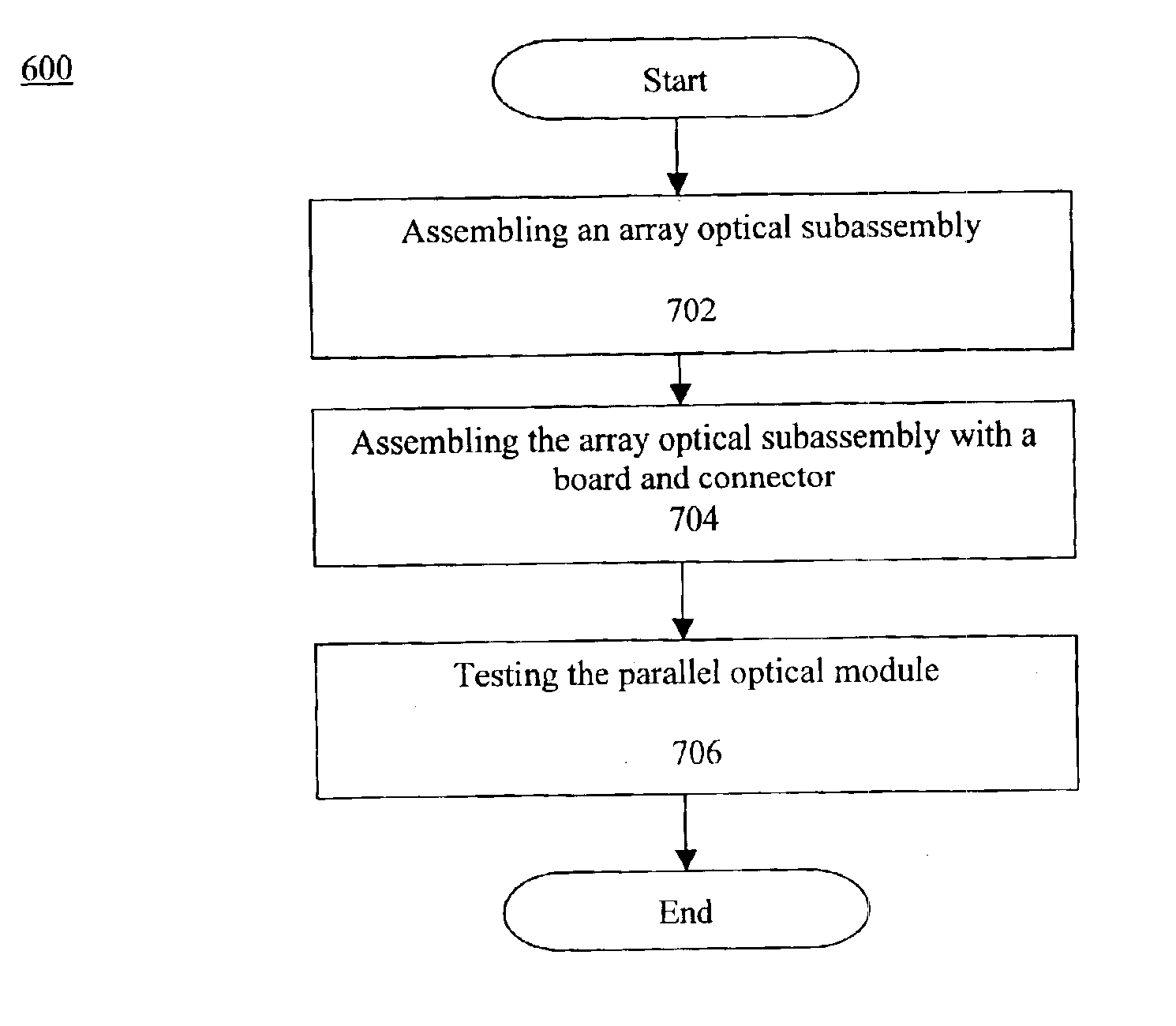
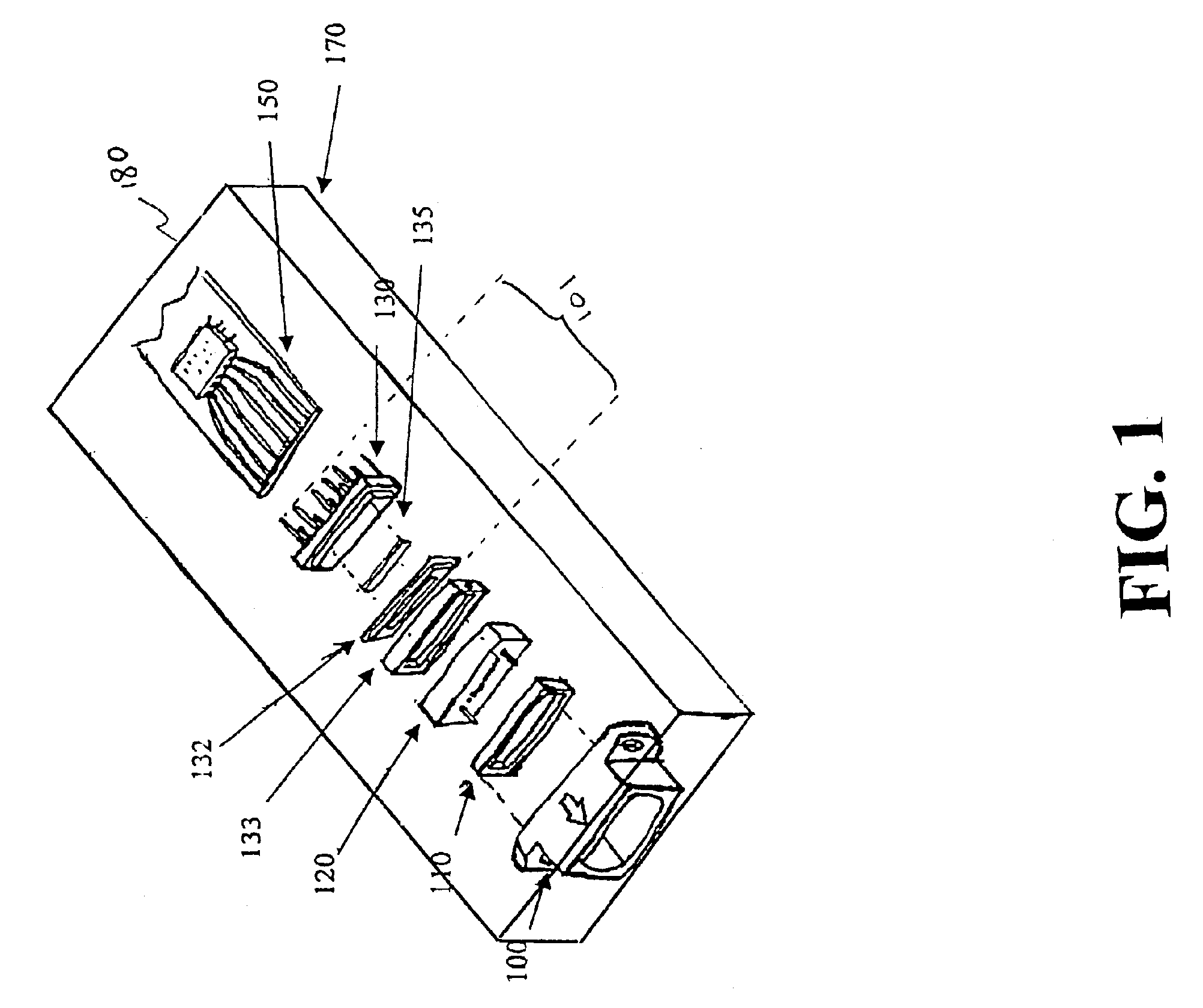
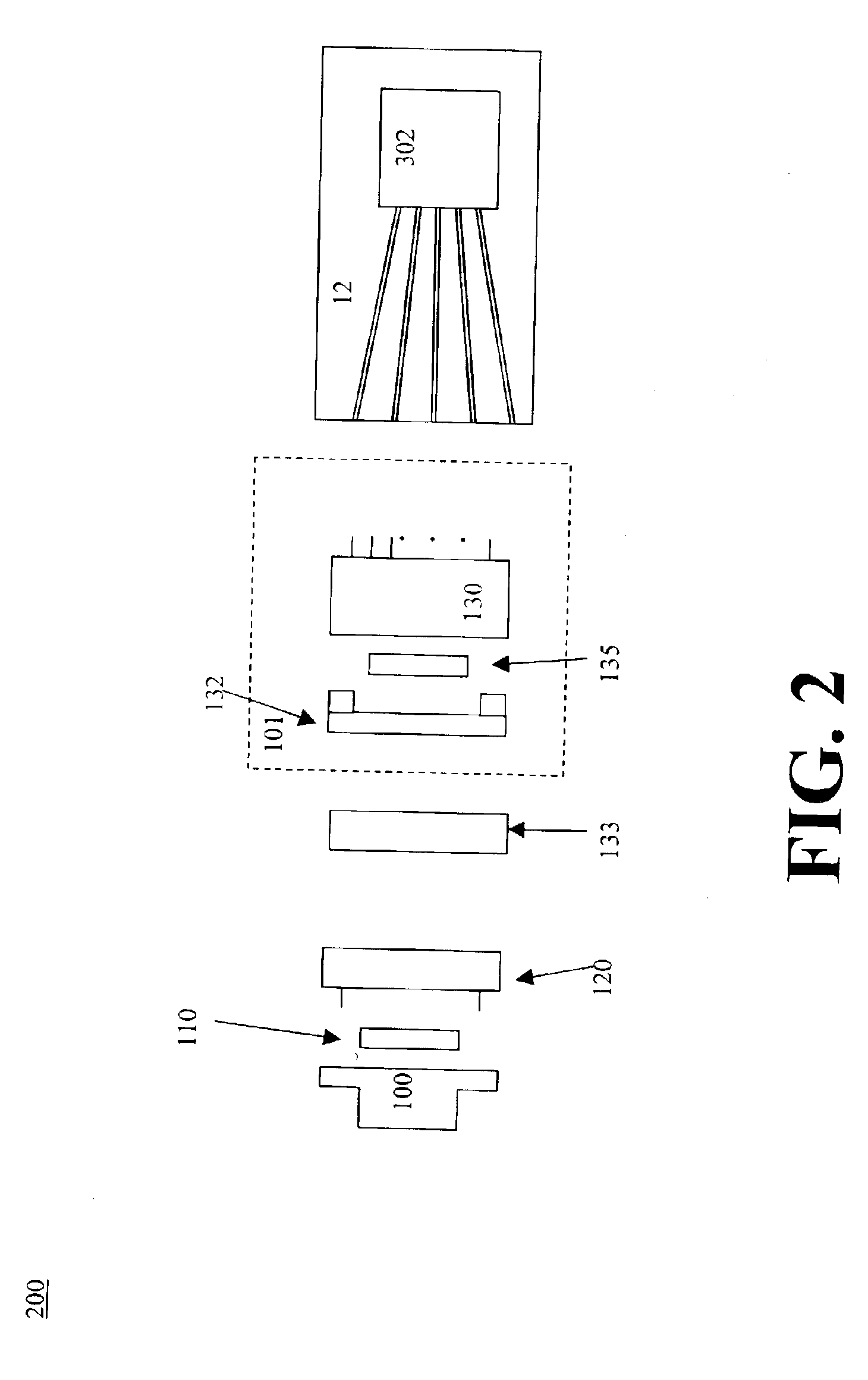
An apparatus and method for manufacturing a parallel optical module, such as a transceiver, transmitter or receiver, using a modular process and hermetically or near-hermetically sealed optoelectronic array devices are discussed.

In the following description, for purposes of explanation, numerous specific details are set forth to provide a thorough understanding of the present invention. It will be apparent, however, to one skilled in the art that these specific details may not be required to practice the present invention. In other instances, well-known circuits and devices are shown in block diagram form to avoid obscuring the present invention.

It is understood that the present invention may contain transistor circuits that are readily manufacturable using well-known art, such as for example CMOS (“complementary metal-oxide semiconductor”) technology, or other semiconductor manufacturing processes. In addition, the present invention may be implemented with other manufacturing proce...


PUM


Abstract

An apparatus and method of modular manufacturing process for a parallel optical transmitter, receiver and/or transceiver is disclosed. The modular process assembles an array of optoelectronic devices to an array header to form an optoelectronic array package. Once the optoelectronic array package is assembled, it is tested and verified the functionality and alignment between the optoelectronic devices and optical fibers. The optoelectronic array package is subsequently coupled to an optical lens array to form an array optical subassembly. After the array optical subassembly is tested, it is coupled to an optical fiber connector to form an optical module. The optical module is then tested to verify its functionality and alignment.

Description

FIELD OF THE INVENTIONThe present invention relates to the field of network communications. More specifically, the present invention relates to a parallel optical transmitter, receiver or transceiver module.BACKGROUNDOptical fibers are one of the most important new media for modern communication to provide very high speed, long-span transmission of information. The fiber optics industry has exploded as the Internet and telecommunication field have created a skyrocketing demand for broadband, high-speed pipelines to carry data. Long-span fiber optic networks of a few hundred kilometers carrying bandwidth ranging from 40 to 50 gigabit per second have been widely deployed. Also, fiber optics plays a very important role in connecting local area networks of 500 meters to 2 kilometers, such as connecting one building to another building. The largest growth area for high-speed fiber optics, however, is connecting distances of less than 300 meters for a wide variety of purposes, including c...

Claims


Application Information

Patent Timeline
Patent Type & Authority Patents(United States)
IPC IPC(8): G02B6/42
CPCG02B6/4249G02B6/4225G02B6/4246
Inventor WANG, CHARLIE X.HOU, HONG Q.MCCORMICK, FREDERICK B.
Owner SUMITOMO ELECTRIC DEVICE INNOVATIONS U S A
Why Eureka
Try Eureka