Charged particle beam exposure method and apparatus
a charge particle and beam technology, applied in the direction of optical radiation measurement, material analysis using wave/particle radiation, instruments, etc., can solve the problems of pattern not being drawn or transferred to the desired position on the wafer, so as to suppress the degradation of drawing accuracy
- Summary
- Abstract
- Description
- Claims
- Application Information
AI Technical Summary
Benefits of technology
Problems solved by technology
Method used
Image
Examples
first embodiment
[First Embodiment]
In this embodiment, an electron beam exposure apparatus using an electron beam will be described as an example of a charged particle beam exposure apparatus. The present invention can also be applied to an exposure apparatus using, e.g., an ion beam as a charged particle beam.
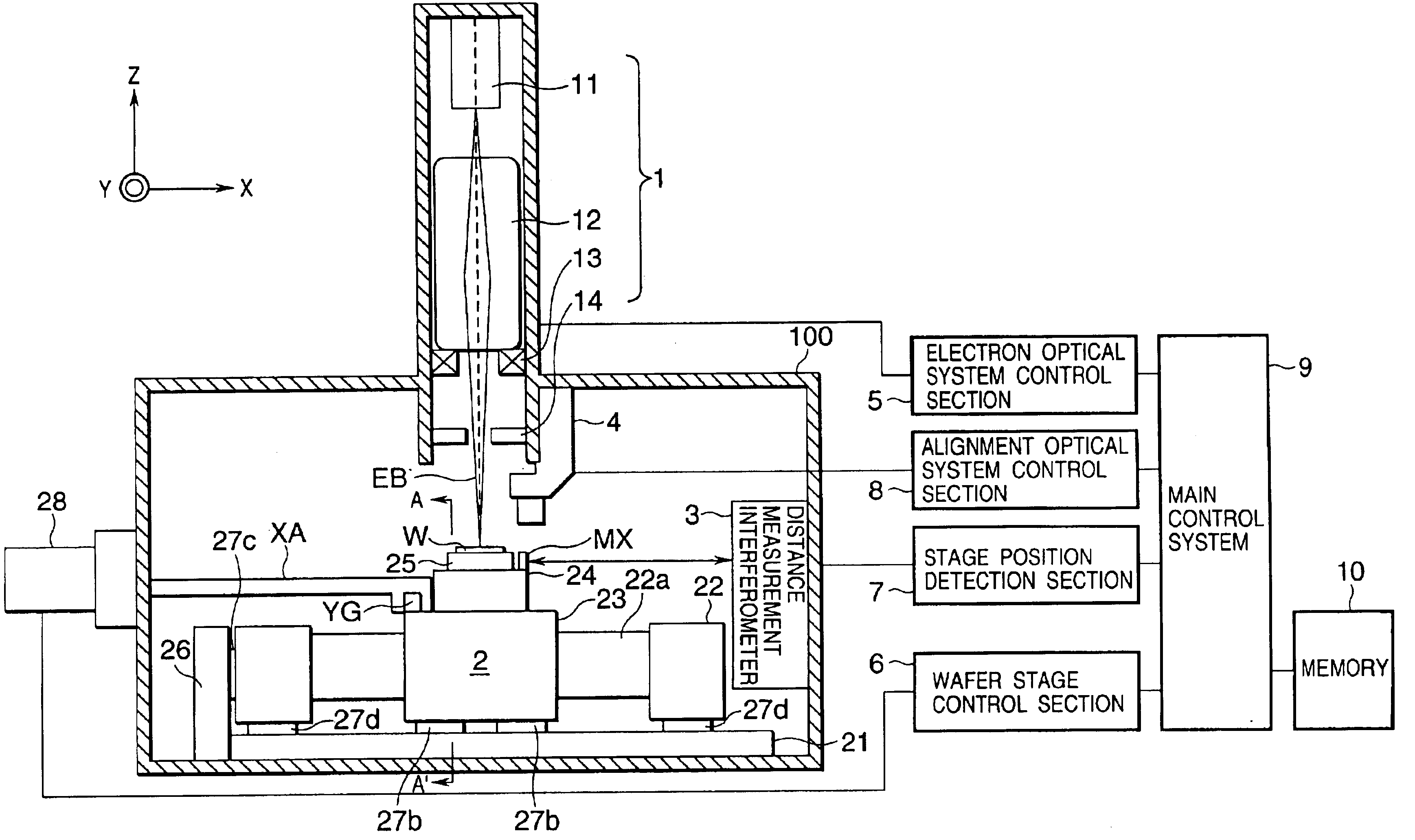
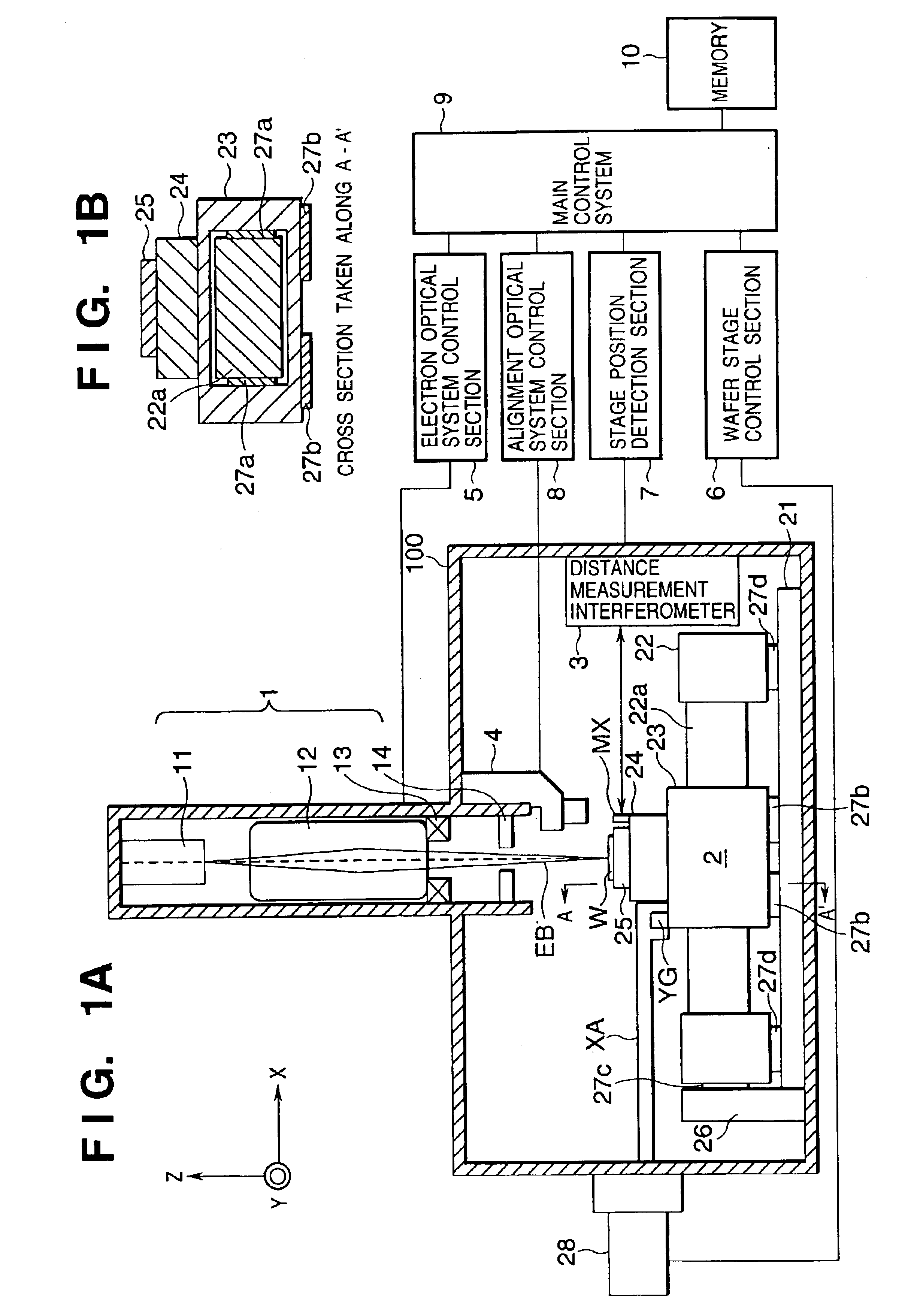
FIGS. 1A and 1B are views showing the arrangement of the electron beam exposure apparatus according to the first embodiment of the present invention.
Referring to FIGS. 1A and 1B, a vacuum chamber 100 is vacuum-evacuated by a vacuum pump (not shown). The vacuum chamber 100 incorporates an electron optical system 1, a wafer stage 2, a distance measurement interferometer 3, an alignment optical system 4, and the like.
The electron optical system 1 has an electron gun 11 for emitting an electron beam, and electron lens system 12 for focusing an electron beam EB from the electron gun 11, a deflector 13 for deflecting the electron beam EB, and an electron detection system 14 for detecting electrons g...
first operation example
FIG. 4 is a flow chart showing the first operation example of the electron beam exposure apparatus according to the first embodiment of the present invention. The first operation example will be described below with reference to FIG. 4.
(Step S101)
A calibration wafer (calibration substrate) is placed on the electrostatic chuck 25 of the wafer stage 2.
The surface of the calibration wafer is coated with a resist. A calibration wafer CW has wafer alignment marks AM1 and AM2, as shown in FIG. 5. The wafer coordinate system on the wafer is defined by the wafer alignment marks AM1 and AM2. The calibration wafer CW is placed on the electrostatic chuck 25 such that the center of the calibration wafer CW, which is defined by the wafer alignment marks AM1 and AM2, is located at the center of the electrostatic chuck 25.
(Step S102)
The wafer alignment marks AM1 and AM2 on the calibration wafer CW are sequentially set under the alignment optical system 4. The position of the X stage 23 at that tim...
second operation example
FIG. 6 is a flow chart showing the second operation example of the electron beam exposure apparatus according to the first embodiment of the present invention. The second operation example will be described below with reference to FIG. 6.
(Step S1101)
The calibration wafer CW (calibration substrate) is placed on the electrostatic chuck 25 of the wafer stage 2.
The calibration wafer CW has a plurality of calibration alignment marks CM, as shown in FIG. 7. As shown in FIG. 7, a reference plate SP having a stage reference mark SM with the same shape as that of the alignment mark AM is fixed on the θ-Z stage 24 of the wafer stage 2. The designed position of the stage reference mark SM in the stage coordinate system is known in advance.
(Step S1102)
On the basis of the designed reference position of the electron optical system 1 and the designed position of the stage reference mark SM, the wafer stage control section 6 controls the wafer stage 2 such that the stage reference mark SM is locate...
PUM
| Property | Measurement | Unit |
|---|---|---|
| electromagnetic field | aaaaa | aaaaa |
| magnetic | aaaaa | aaaaa |
| imaging characteristics | aaaaa | aaaaa |
Abstract
Description
Claims
Application Information


