Thermal-assisted switching array configuration for MRAM

Active Publication Date: 2005-03-08
SAMSUNG ELECTRONICS CO LTD
View PDF9 Cites 21 Cited by
  • Summary
  • Abstract
  • Description
  • Claims
  • Application Information

AI Technical Summary

Benefits of technology

In particular, and by way of example only, according to an embodiment of the present invention, this invention provides a thermal-assisted magnetic memory storage device including: a cross point array of magnetic tunnel junction memory cells, the memory cells characterized by a material wherein the coercivity is decreased upon an increase in temperature; a plurality of separate looping write conductors positioned within close proximity about each magnetic tunnel junction memory cell.
Moreover, according to an embodiment thereof, the invention may provide a thermal-assisted magnetic memory storage device including: a plurality of parallel electrically conductive rows; a plurality of parallel electrically conductive columns transverse to the rows, the columns and rows thereby forming a cross point array with a plurality of intersections; a plurality of offset magnetic tunnel junction memory cells, each memory cell located proximately to and in electrical contact with an intersection between a row and column, the memory cells characterized by a material with an alterable orientation of magnetization, wherein the coercivity of the alterable material is decreased upon an increase in temperature; and a plurality of separate looping write conductors positioned within close proximity about each magnetic tunnel junction memory cell.
In yet another embodiment, the invention may provide a thermal-assisted magnetic memory storage device including: a plurality of parallel electrically conductive rows; a plurality of parallel electrically conductive columns transverse to the rows, the columns and rows thereby forming a cross point array with a plurality of intersections; a plurality of offset magnetic tunnel junction memory cells, each memory cell located proximately to and in electrical contact with an intersection between a row and column, each memory cell including: a top offset electrical conductor joined to the row and extending substantially transversely from the row for a length at least the width of the memory cell; at least one

Problems solved by technology

Main memory is generally comprised of fast, expensive volatile random access memory that is connected directly to the processor by a memory bus.
This offset can result in asymmetry in the switching characteristics of the bit: the amount of switching field needed to switch the bit from parallel to anti-parallel state is different from the switching field needed to switch the bit from anti-parallel state to parallel state.
Thus, at least one disadvantage of a tunnel junction memory cell having a pinned reference layer in close and fixed proximity to the data layer is a potential reduction in the magneto-resistance ΔR/R resulting from the angular displacement.
Such manufacturing stresses may permit the reference layer to become un-pinned and lose it's set orientation if the memory is later subjected to high temperatures.
In addition, the characteristics of th

Method used


Image

  • Thermal-assisted switching array configuration for MRAM
  • Thermal-assisted switching array configuration for MRAM
  • Thermal-assisted switching array configuration for MRAM

Examples


Embodiment Construction

Before proceeding with the detailed description, it is to be appreciated that the present invention is not limited to use or application with a specific type of magnetic memory. Thus, although the present invention is, for the convenience of explanation, depicted and described with respect to typical exemplary embodiments, it will be appreciated that this invention may be applied with other of magnetic memory.

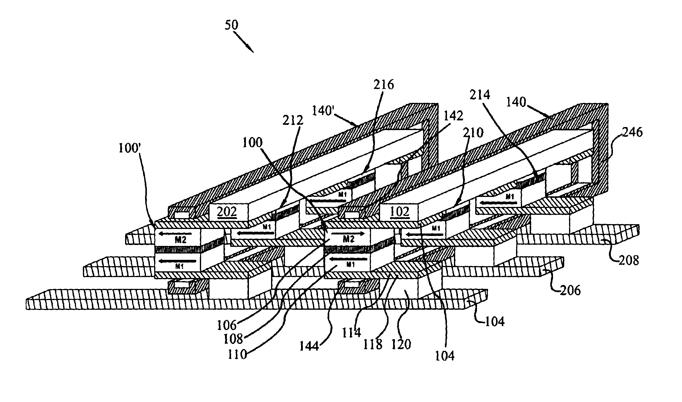
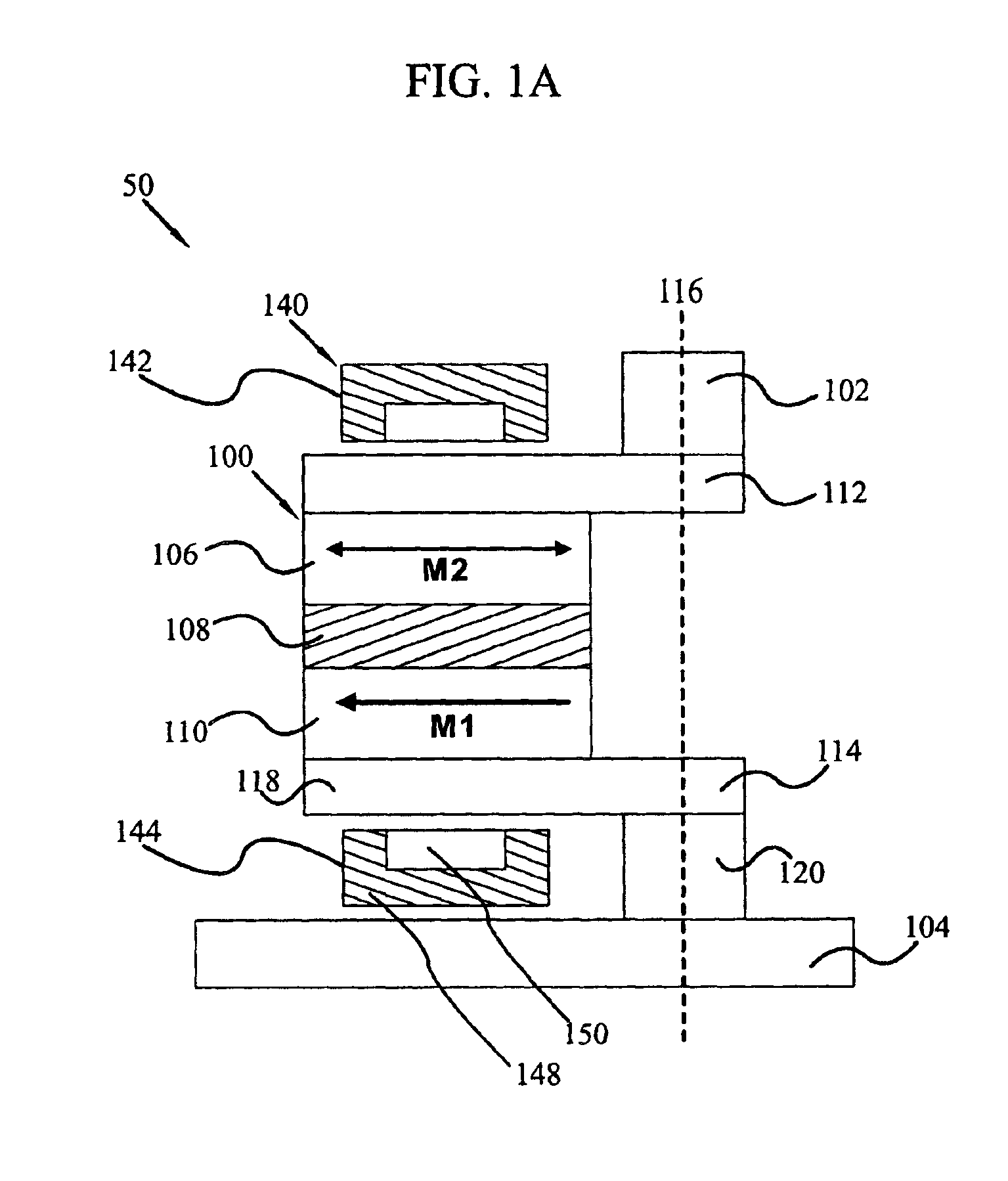
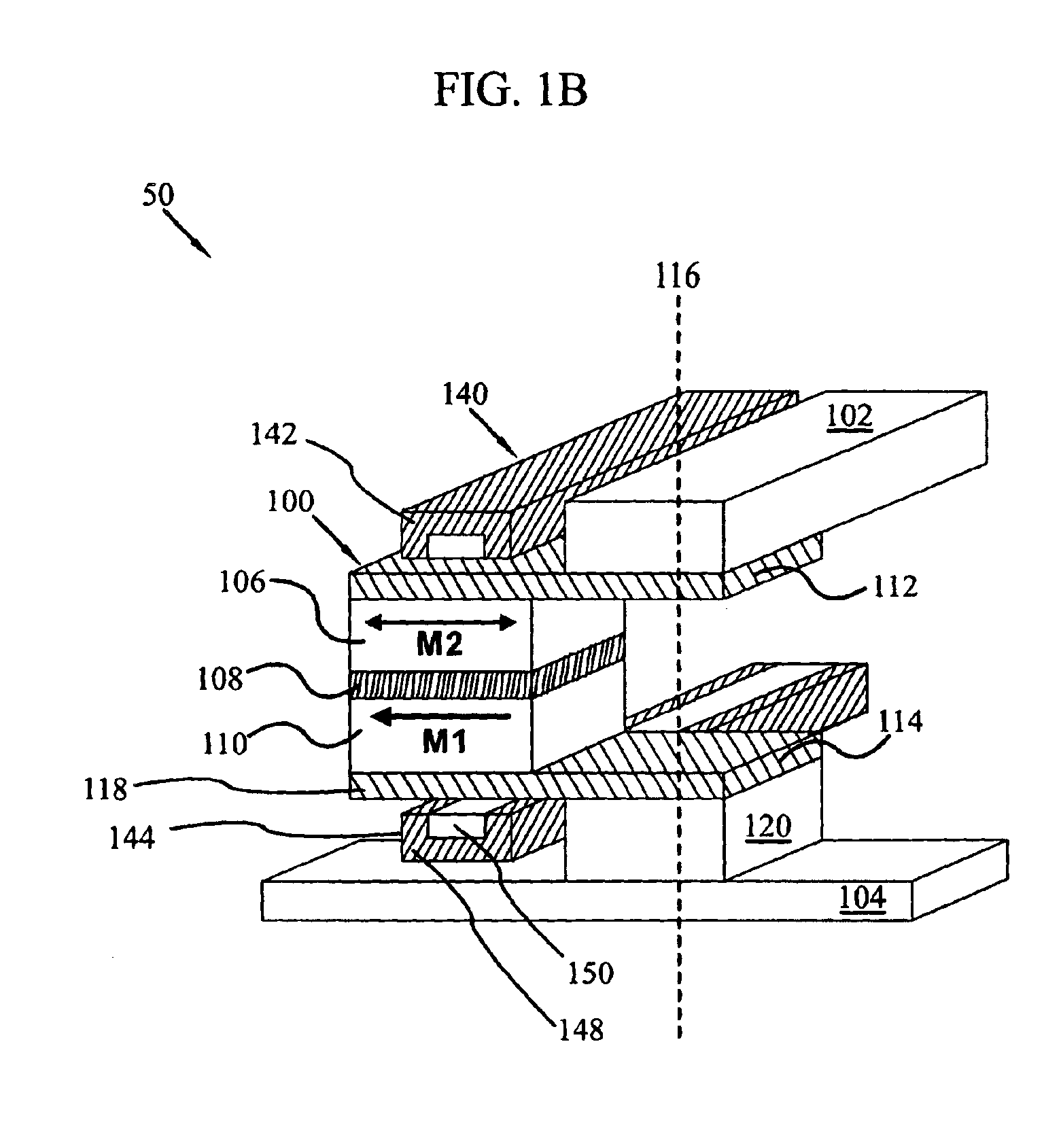
Referring now to the drawings, and more particularly to FIG. 1A and the perspective of FIG. 1B, there is shown a portion of a thermal-assisted switching magnetic memory 50, having at least one magnetic memory cell 100 and at least one separate looping write conductor 140, positioned proximate to the memory cell 100, according to an embodiment of the present invention. In at least one embodiment, the magnetic memory cell 100 may be a magnetic memory tunnel junction memory cell. Specifically, the memory 50 provides a plurality of parallel electrically conductive rows and parallel...


PUM


Abstract

This invention provides a thermal-assisted switching magnetic memory storage device. In a particular embodiment, a cross-point array of conductive rows and columns is provided with offset tunnel junction magnetic memory cells provided proximate to the intersections between the rows and columns. A looping write conductor is provided close to, but not in electrical contact with each memory cell. The looping write conductor loops across the top and bottom of each memory cell. Each magnetic memory cell provides a magnetic data layer characterized by a material wherein the coercivity is decreased upon an increase in temperature, an intermediate layer, and a reference layer. The magnetic fields provided by the looping write conductor during a write operation are not sufficient to alter the magnetic orientation of an unheated data layer, but may alter the data layer of a memory cell warmed by a bias current tunneling through the memory cell.

Description

FIELD OF THE INVENTIONThis invention relates generally to magnetic memory devices and in particular to ultra-high density thermally assisted magnetic random access memory arrays (commonly referred to as “MRAM”).BACKGROUND OF THE INVENTIONToday's computer systems are becoming increasingly sophisticated, permitting users to perform an ever greater variety of computing tasks at faster and faster rates. The size of the memory and the speed at which it can be accessed bear heavily upon the overall speed of the computer system.Memory for a computer system is technically any form of electronic, magnetic or optical storage; however it is generally divided up into different categories based in part upon speed and functionality. The two general categories of computer memory are main memory and mass storage. Main memory is generally comprised of fast, expensive volatile random access memory that is connected directly to the processor by a memory bus. One component of the speed in main memory i...

Claims


Application Information

Patent Timeline
IPC IPC(8): G11C11/15G11C11/02H01L21/8246H01L27/105H01L43/08
CPCG11C11/15
Inventor TRAN, LUNG T.
Owner SAMSUNG ELECTRONICS CO LTD
Why Eureka
Try Eureka