Mixer having low noise, controllable gain, and/or low supply voltage operation
- Summary
- Abstract
- Description
- Claims
- Application Information
AI Technical Summary
Problems solved by technology
Method used
Image
Examples
Embodiment Construction
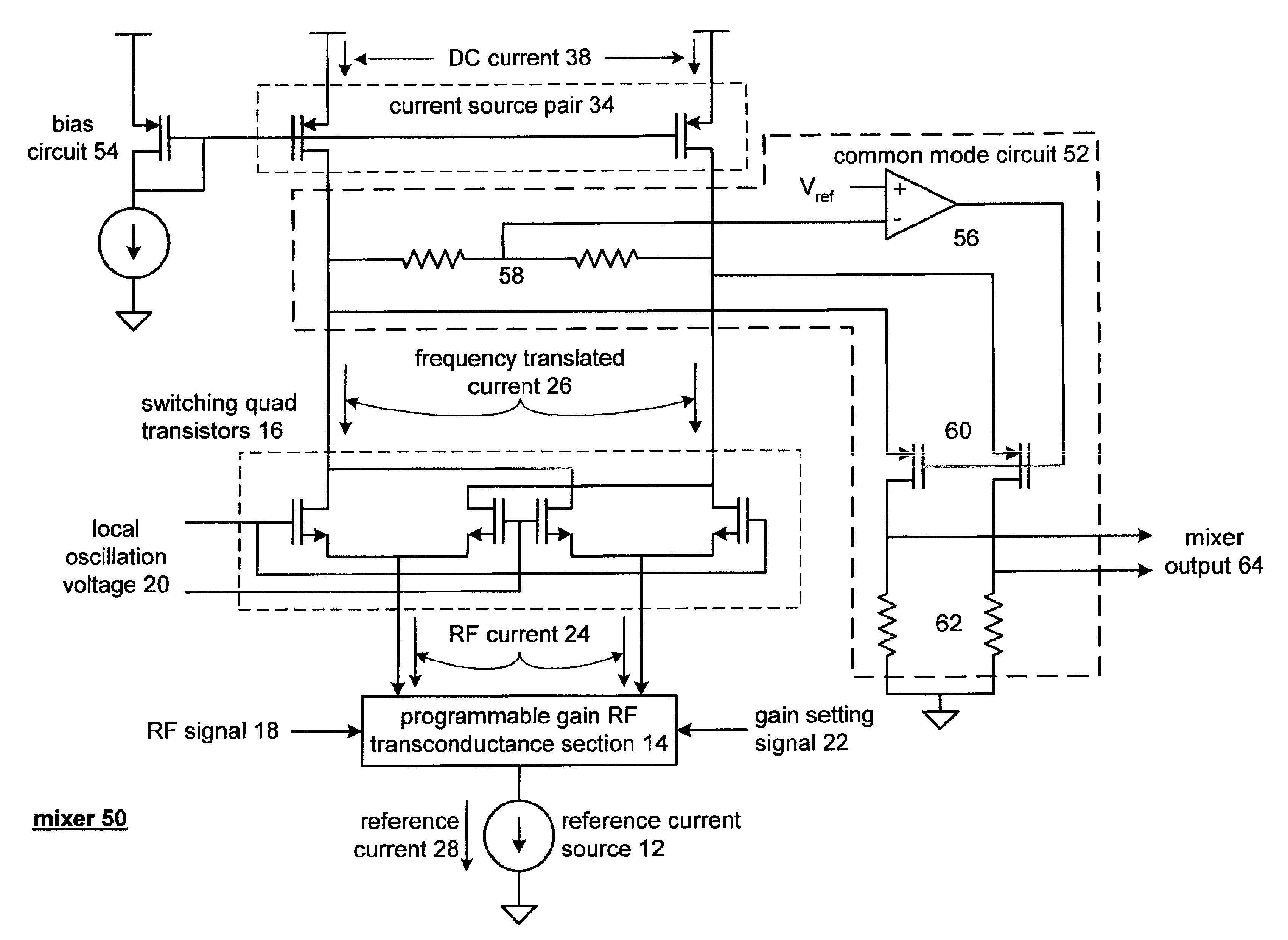
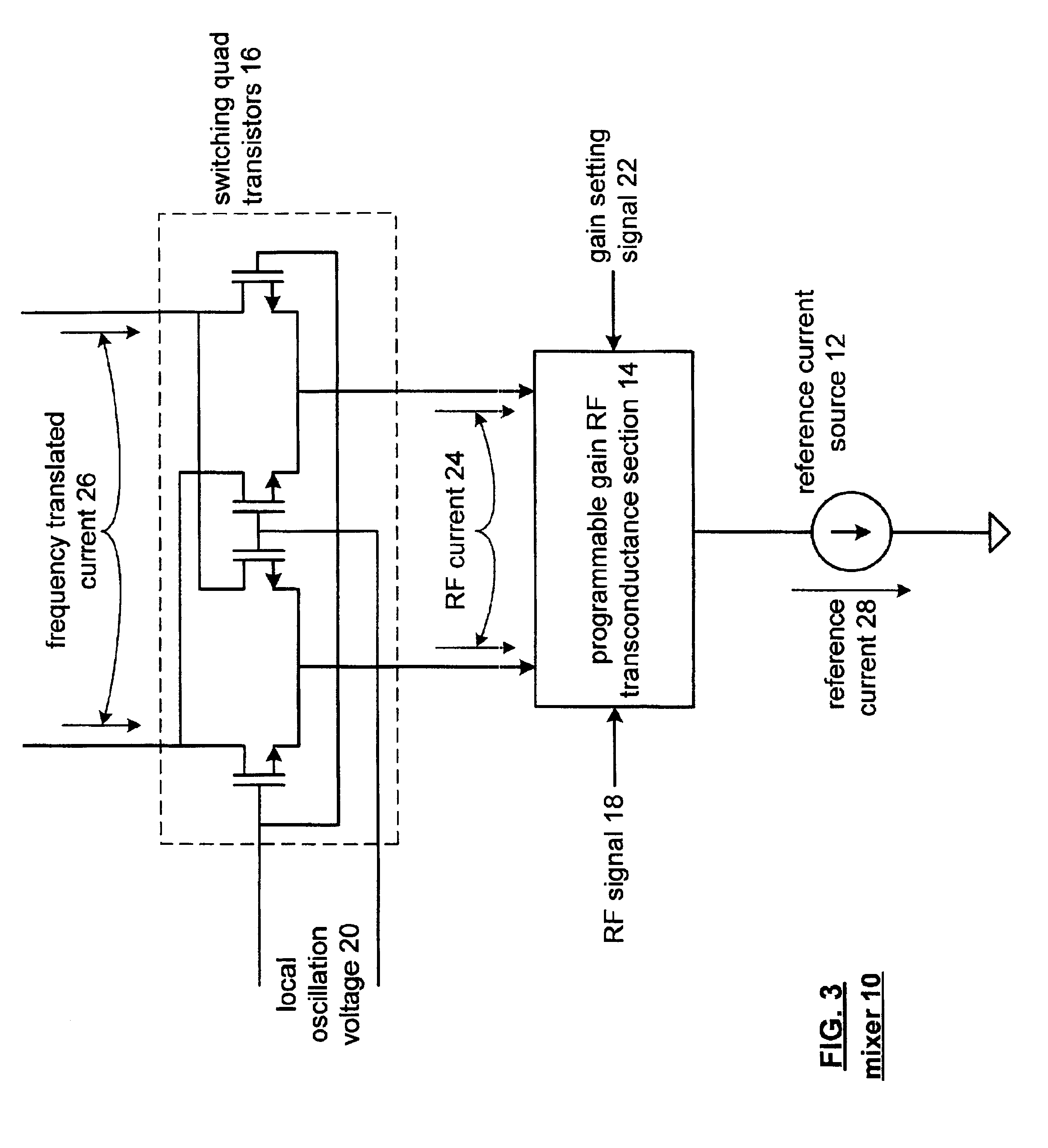
FIG. 3 illustrates a schematic block diagram of a mixer 10 that includes a reference current source 12, a programmable gain RF transconductance section 14, and switching quad transistors 16. The reference current source 12 is operably coupled to provide a reference current 28 to the programmable gain RF transconductance section 14. The programmable gain RF transconductance section 14, which will be described in greater detail with reference to FIGS. 8 and 9, receives a RF signal 18 and a gain setting signal 22. Based on these inputs and the reference current 28, the programmable gain RF transconductance section 14 produces an RF current 24. Accordingly, the RF current 24 is representative of the RF signal 18 amplified in accordance with the gain setting signal 22.
The switching quad transistors 16 are operably coupled to generate a frequency translated current 26 from a local oscillation voltage 20 and the RF current 24. Accordingly, the frequency translated current 26 represents an ...
PUM
 Abstract
Description
Claims
Application Information


