Semiconductor integrated circuit device including a substrate bias controller and a current limiting circuit

a technology of current limiting circuit and integrated circuit device, which is applied in the direction of pulse manipulation, pulse technique, instruments, etc., can solve the problems of wasteful current consumption for generating back gate voltage, lower voltage conversion efficiency, and relative large power consumption of the devi

Inactive Publication Date: 2005-03-15
RENESAS ELECTRONICS CORP
View PDF10 Cites 51 Cited by
  • Summary
  • Abstract
  • Description
  • Claims
  • Application Information

AI Technical Summary

Problems solved by technology

This charge pump circuit is so-called a DC-DC converter, however a voltage conversion efficiency is lower, then the power consumption thereof comes to be relative large.
In the prior art 1 mentioned above, when having the plural number of operation modes, as was mentioned in the above, it comes to be large in circuit scale (i.e., the number of transistors in the circuit), due to the necessity of the number of the voltage generators corresponding to them, and in such one, in which the back gates are generated corresponding to the plural number of the operation modes, as was mentioned in the above, on the contrary to that the necessary back gate is only one (1) in one (1) operation mode, there is a problem that wasteful consumption of current occurs for generating the back gate voltages which are not used.
Then, it is sufficient that only the voltage generator corresponding thereto is operated when having only one (1) operation mode, while stopping the operation of the voltage generators corresponding to the other back gate voltages, however in such the case, it follows a victim of loosing a responsibility in changing over the operation modes.

Method used


Image

  • Semiconductor integrated circuit device including a substrate bias controller and a current limiting circuit
  • Semiconductor integrated circuit device including a substrate bias controller and a current limiting circuit
  • Semiconductor integrated circuit device including a substrate bias controller and a current limiting circuit

Examples


Embodiment Construction

A description will be given of the present invention embodiments by reference to the accompanying drawings.

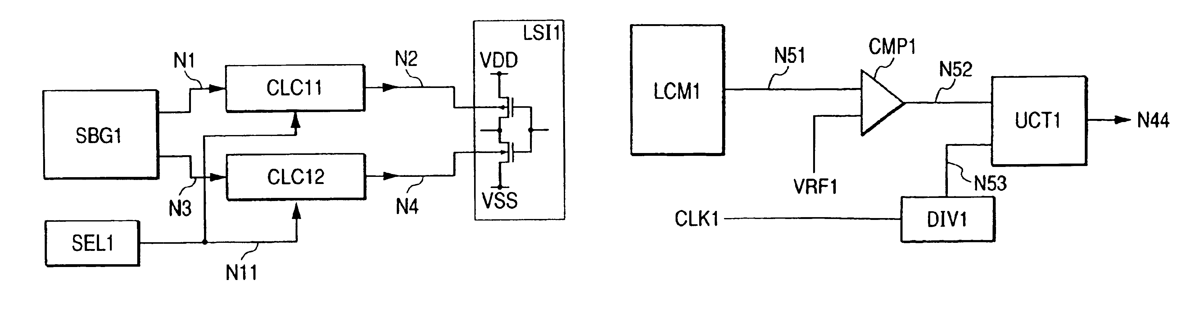
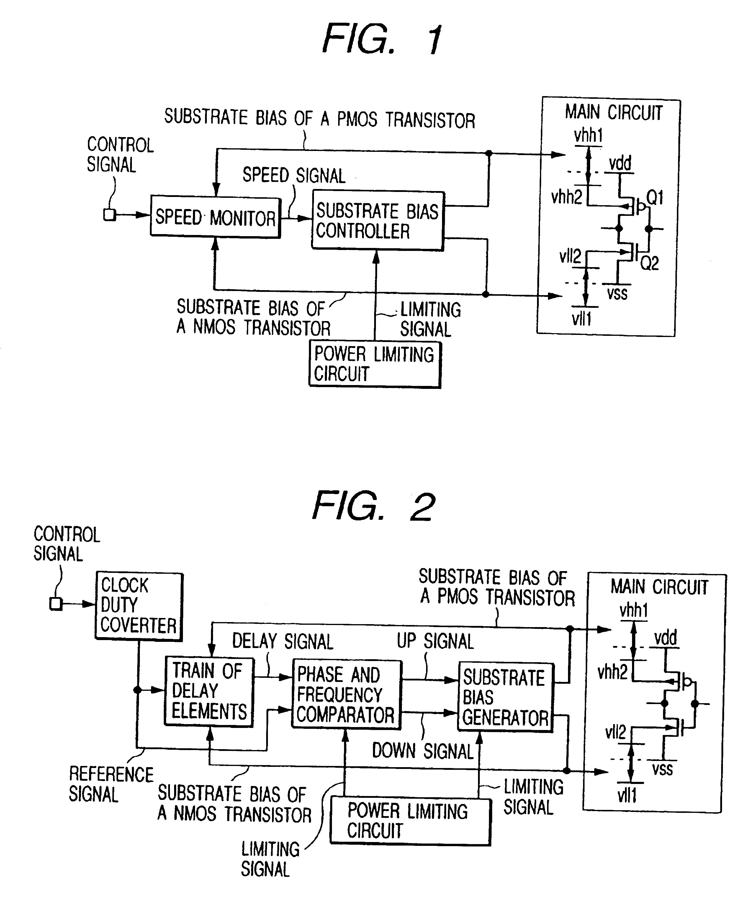
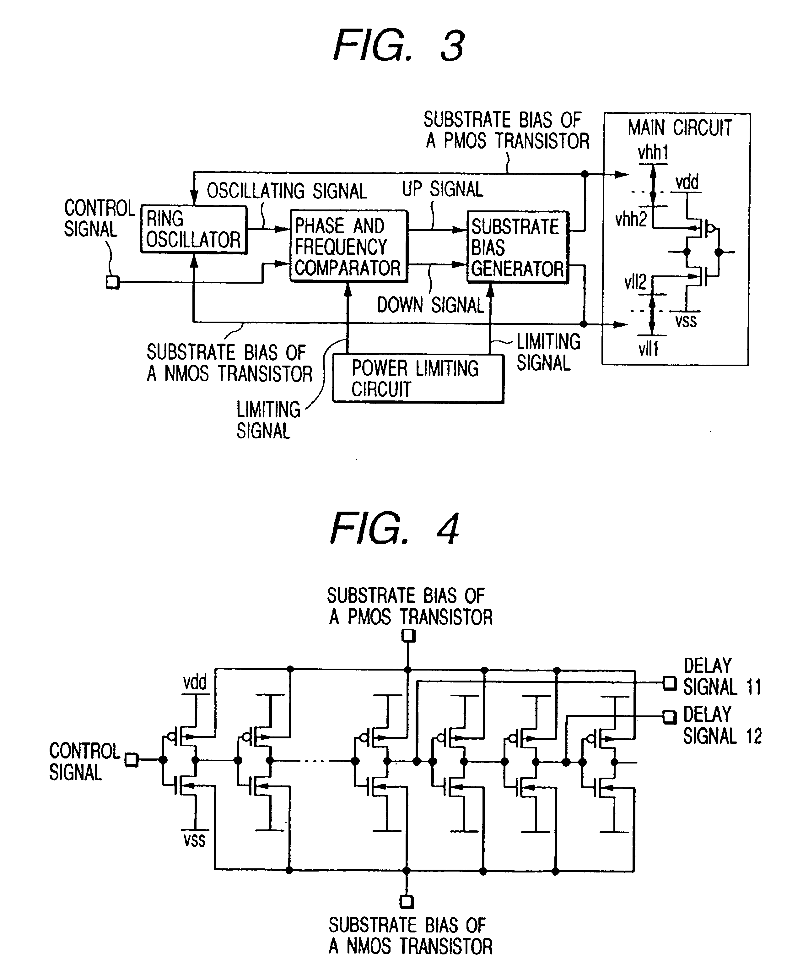
In FIG. 1 is shown a basic block diagram of an embodiment of a semiconductor integrated circuit, according to the present invention. In the same figure, circuit block(s) relating to the present invention is / are taken out to be shown therein. Each of the circuit block(s), although should not be restricted only thereto in particular, it is formed on one (1) piece of a semiconductor substrate, such as a single crystal silicon, through a manufacturing technology for a conventional CMOS integrated circuit.

In the present application, essentially, a terminology “MOS” should be understood to call for or refer to the structure of metal oxide semiconductor in brief. However, the MOS in accordance with a general reference thereof in recent years, includes one, in which a metal portion essential to the semiconductor device is replaced by an electric conductive material other than metals, s...


PUM


Abstract

In a semiconductor integrated circuit device, for realizing high speed, as well as superior product yield rate and usability, while reducing circuit scale and improving on product yield rate and reliability thereof, a main circuit, constructed with CMOS elements, is coupled to a speed monitor circuit for forming a speed signal corresponding to an operating speed thereof and to a substrate bias controller for supplying corresponding substrate bias voltages to the main circuit in response to the speed monitor circuit. A current limiting circuit is also provided in conjunction with the substrate bias controller to prevent an overflow of current due to bias voltage.

Description

FIELD OF THE INVENTIONThe present invention relates to a semiconductor circuit device, and in particular relates to a technology, being effective when applied onto a MOS circuit which is operated at a plural number of operating speeds, or when applied onto a MOS circuit on which high speed operation is required.BACKGROUND OF THE INVENTIONDue to a search made after accomplishing the present invention, though will be explained later, it appears that there is known Japanese Patent Laying-Open. No. 11-122047 (1999) (hereinafter, prior art 1), as a prior art seeming to be relevant thereto. In the patent Laying-Open of the prior art 1, for the purpose of reducing current consumption without deteriorating the process performance or property thereof, a voltage level of a back gate voltage, which is applied to a back gate of a MOS transistor contained within an interior circuit, is supplied by selecting an output voltage from a voltage generator for generating a plurality of voltages, being ...

Claims


Application Information

Patent Timeline
Patent Type & Authority Patents(United States)
IPC IPC(8): G05F3/20G05F3/08H01L27/04G11C11/34G11C11/408H01L21/822H01L21/8238H01L27/092H03K5/135H03K19/094H03M1/66
CPCG05F3/205G11C11/34
Inventor MIYAZAKI, MASAYUKIISHIBASHI, KOICHIROONO, GOICHI
Owner RENESAS ELECTRONICS CORP
Why Eureka
Try Eureka