Multi-level stamper for improved thermal imprint lithography

Inactive Publication Date: 2005-03-22
SEAGATE TECH LLC
View PDF2 Cites 82 Cited by
  • Summary
  • Abstract
  • Description
  • Claims
  • Application Information

AI Technical Summary

Benefits of technology

An advantage of the present invention is an improved method of performing thermal imprint lithography of a substrate/workpiece surface, wherein random formation of undesired, disordered features in portions of the surface where features are not intended to be formed, is substantially prevented.
Another advantage of the present invention is an improved method of performing thermal imprint lithography of a substrate/workpiece surface, wherein pattern destruction resulting from shear forces arising from relative movement between the stamper/imprinter utilized for pattern imprinting and the substrate/workpiece during thermal cycling between lower and higher temperatures is substantially prevented.
Yet another advantage of the present invention is an improved, multilevel stamper/imprinter for use in performing thermal imprint lithography of a substrate/workpiece surface, wherein random formation of undesired, disordered features in portions of the surface where features are not intended to be formed, is substantially prevented.
Still another advantage of the present invention is an improved multilevel, shallow-grooved stamper/imprinter for use in performing thermal imprint lithography of a substrate/workpiece surface wherein pattern destruction resulting from shear forces arising from relativ

Problems solved by technology

However, the constantly increasing demands of micro-miniaturization for increased data storage and computation require fabrication of devices with ever smaller dimensions, which demands tax or even exceed the limits of conventional optical lithographic patterning processes utilizing visible light.
However, while each of these techniques is capable of providing high resolution, finely-dimensioned patterns and features, the economics of their use is less favorable, due to such factors as limitations arising from wavelength-dependent phenomena, slow e-beam and SP writing speeds, and difficulties in the development of suitable resist materials.
However, two significant problems have been encountered with the use of the above-described thermal imprint lithography technique when utilized w

Method used


Image

  • Multi-level stamper for improved thermal imprint lithography
  • Multi-level stamper for improved thermal imprint lithography
  • Multi-level stamper for improved thermal imprint lithography

Examples


Example

EXAMPLE

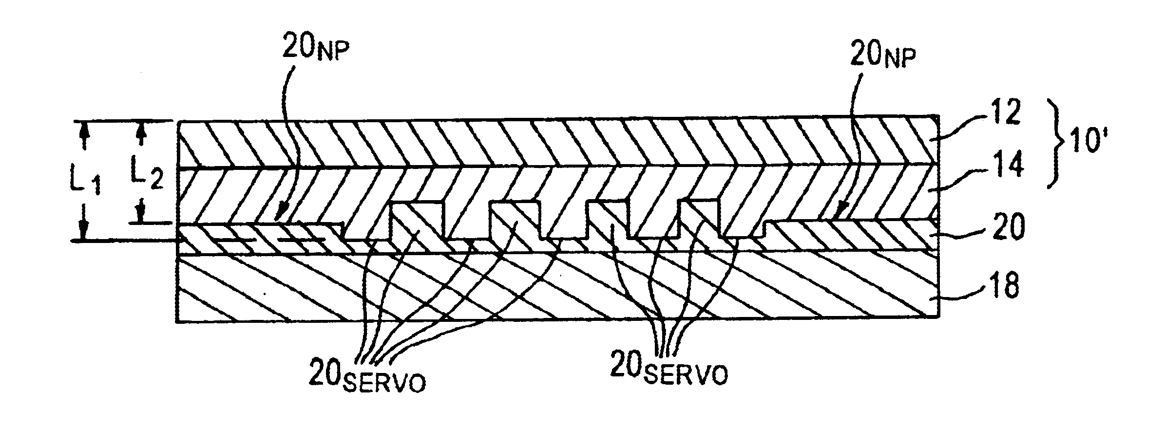
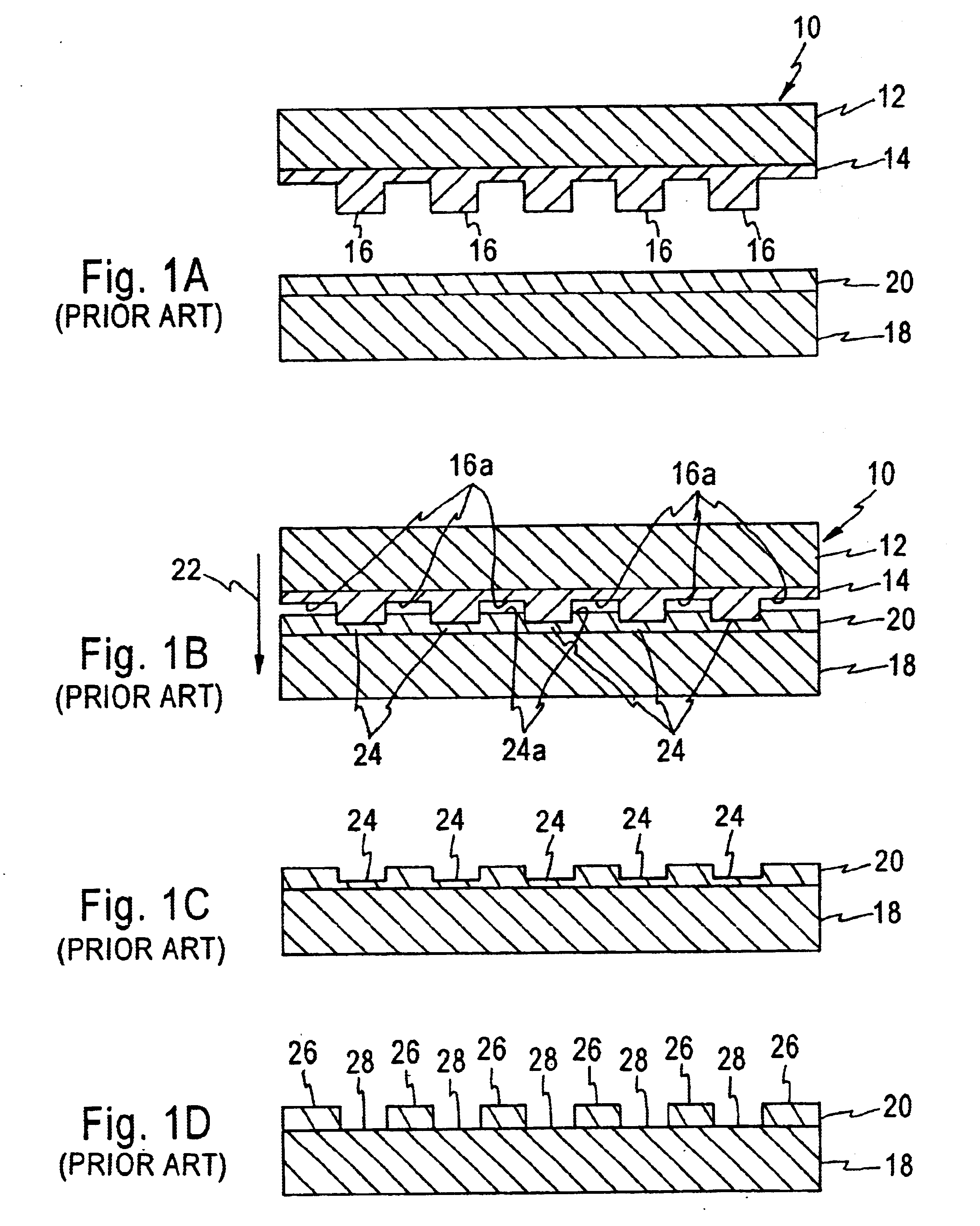
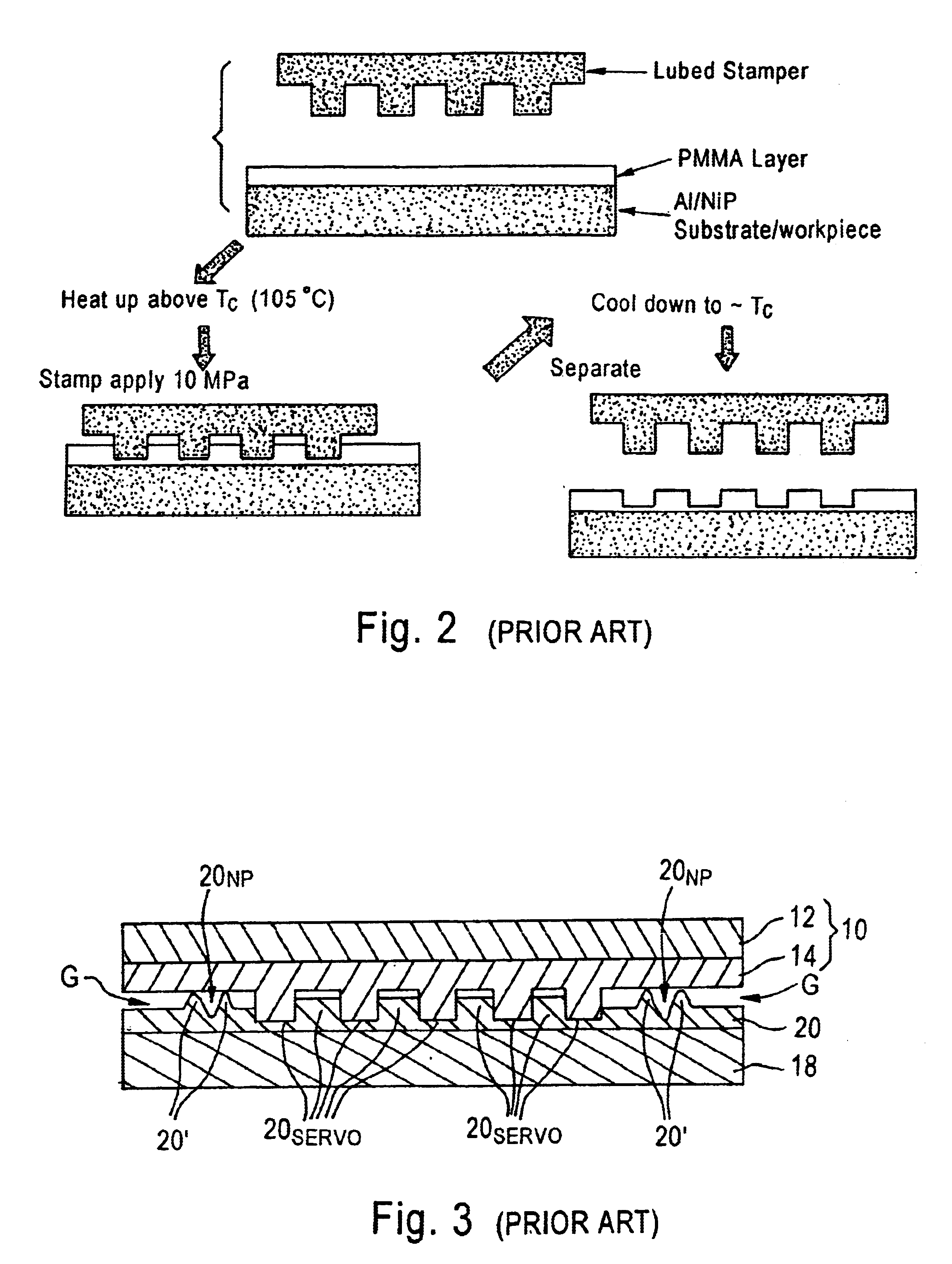
Shallow-grooved, multilevel stampers / imprinters 10″ as shown in FIG. 5 were fabricated by means of a laser beam exposure apparatus and Ni electroplating. The shallow grooves 20SG were patterned on a photoresist layer using a lower exposure dose than that used for patterning the full height (or depth) features 20SERVO of the servo pattern portion of the imprinting surface. Ni was electroplated on the patterned photoresist to replicate the resist pattern. Several generations of stampers / imprinters 10″ were fabricated by successive electroplating of the patterned photoresist. Servo patterns were stamped / imprinted onto PMMA-coated, Al disk substrates at about 140° C. and released therefrom at about 120° C. Excellent replication fidelity was obtained, as determined by scanning probe AFM measurements. Further, the excellent replication fidelity was obtained despite the use of the Ni-based stampers / imprinters 10″, which have a different thermal expansion characteristic than that of ...


PUM

PropertyMeasurementUnit
Temperatureaaaaaaaaaa
Levelaaaaaaaaaa

Abstract

A stamper/imprinter for use in performing thermal imprint lithography of a substrate/workpiece surface to form a pattern of features in first portions of the surface intended to receive the pattern, without incurring random formation of undesired, disordered features in second portions of the substrate/workpiece surface not intended to receive the pattern, comprising an imprinting surface configured to substantially prevent formation of gaps between the imprinting surface and the second portions of the surface during stamping/imprinting. Embodiments include stampers/imprinters with a multilevel imprinting surface comprises a first portion having a first level for forming the pattern of features in the first portions of the surface and a second portion having a second level for substantially preventing formation of gaps between the imprinting surface and the second portions of the surface during stamping/imprinting.

Description

FIELD OF THE INVENTIONThe present invention relates to methods and apparatus for forming sub-micron sized features and patterns in large area substrate surfaces by means of thermal imprint lithography. The invention has particular utility in the formation of servo patterns in the surfaces of substrates utilized in the manufacture of data / information storage and retrieval media, e.g., hard disk magnetic media.BACKGROUND OF THE INVENTIONOptical-based lithographic techniques are widely employed in the fabrication of integrated circuits (ICs) and other devices requiring very fine-dimensioned patterns or features. However, the constantly increasing demands of micro-miniaturization for increased data storage and computation require fabrication of devices with ever smaller dimensions, which demands tax or even exceed the limits of conventional optical lithographic patterning processes utilizing visible light. As a consequence, intense research has been conducted on ultra-violet (UV), X-ray...

Claims


Application Information

Patent Timeline
IPC IPC(8): B29C59/00B29D17/00G03F7/00
CPCB82Y10/00G11B5/855G03F7/0002B82Y40/00
Inventor WAGO, KOICHIGAUZNER, GENNADYFORMATO, CHRISTOPHER JOSEPH
Owner SEAGATE TECH LLC
Why Eureka
Try Eureka