

Wiring board with core layer containing inorganic filler
- Summary
- Abstract
- Description
- Claims
- Application Information
AI Technical Summary
Benefits of technology
Problems solved by technology
Method used
Image

Examples
example 1
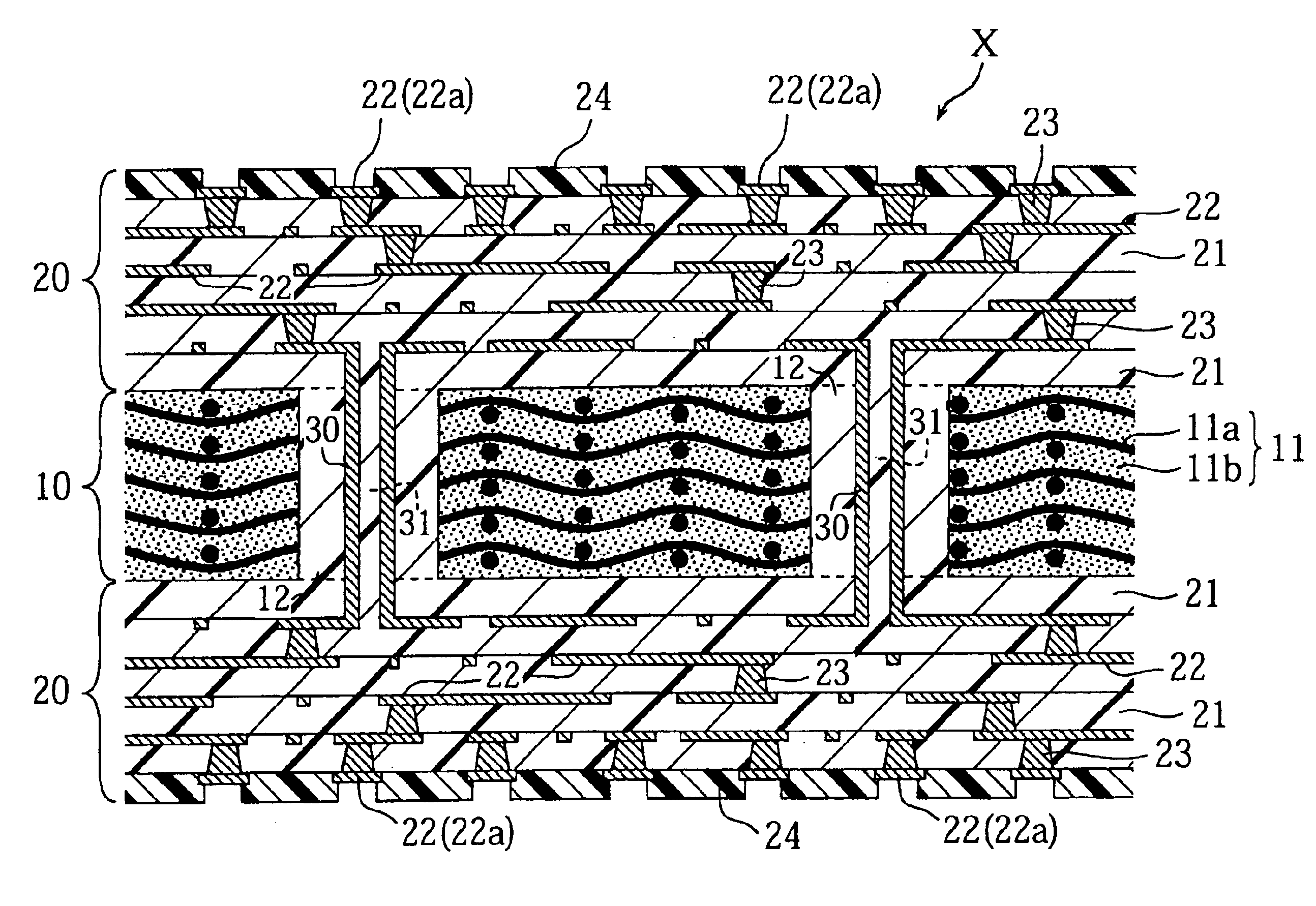
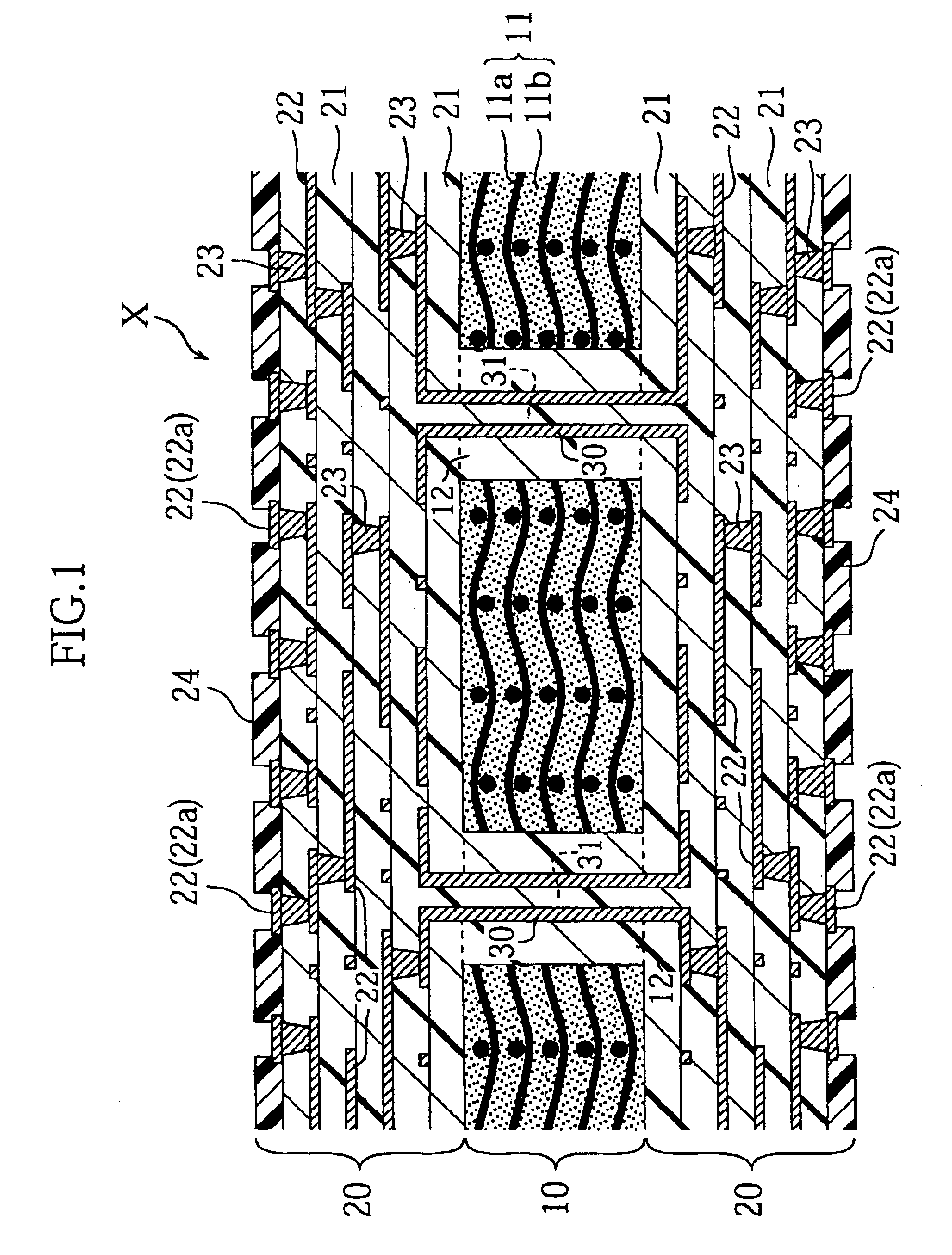
[0056]
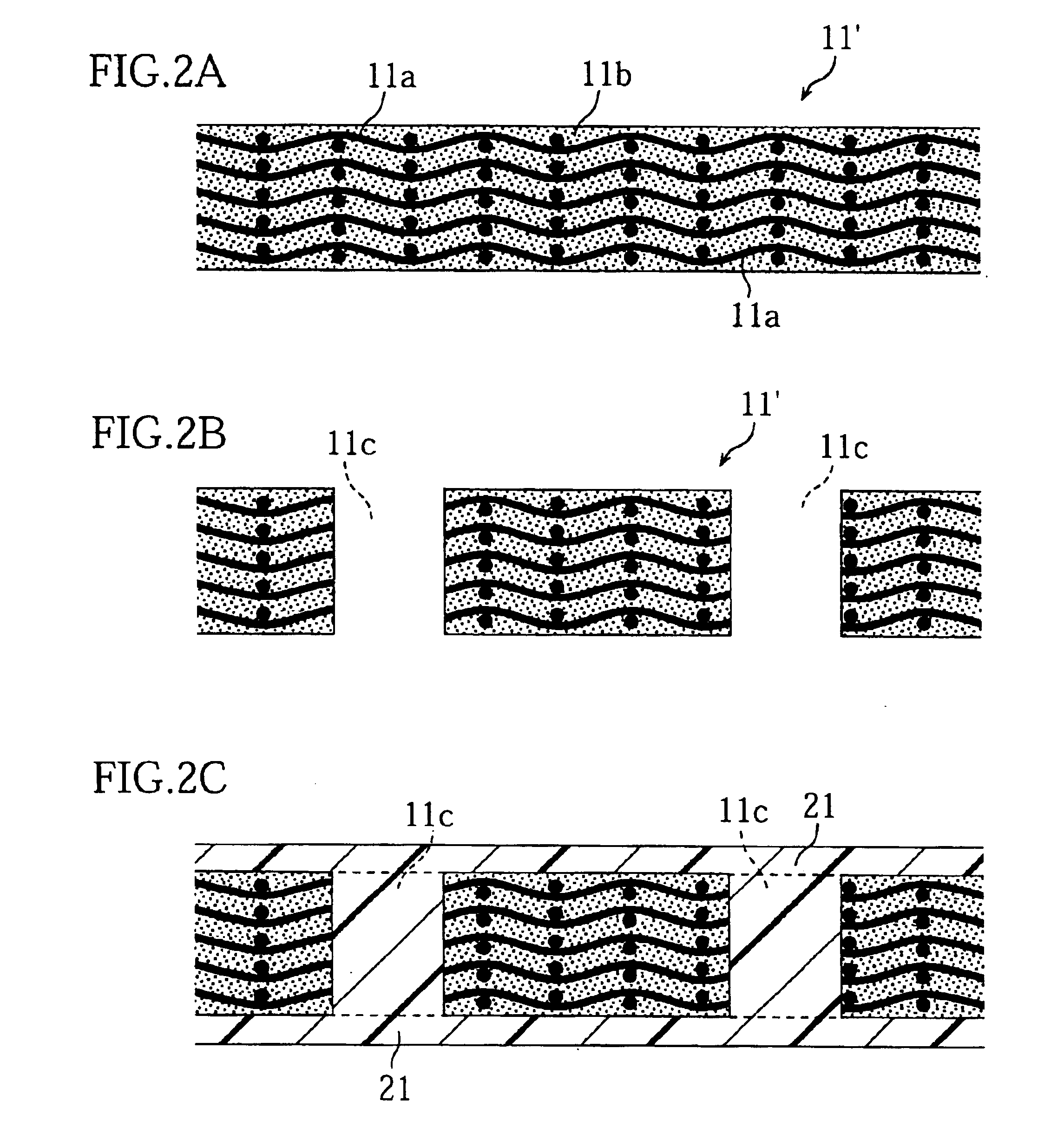
[0057]In this example, the CFRP plate was formed from carbon fiber cloth and a polyimide resin composite. The CFRP plate was produced in the following manner. First, carbon fiber cloth (Brand name: TORAYCA manufactured by Toray Industries Inc.) was impregnated with a thermosetting polyimide resin composite and then dried to provide a prepreg having a thickness of 0.2 mm. The carbon fiber cloth was a flat-woven material formed from carbon fiber threads each made by bundling 200 or more carbon fibers (each fiber has a diameter not greater than 10 μm). Before hardened, the polyimide resin composite contained monomers (for forming the polymer), a hardener, and inorganic fillers such as alumina powder (no greater than 7 μm in weight average particle size) and silica powder (no greater than 3 μm in weight average particle size). The polyimide resin composite contained a 10 wt % of alumina powder and a 10 wt % of silica powder. The thermal expansion coefficient of the alumina powder ...
example 2
[0067]
[0068]In this example, the CFRP plate was formed from carbon fiber cloth and an epoxy resin composite. The CFRP plate was produced in the following manner. First, carbon fiber cloth (Brand name: TORAYCA manufactured by Toray Industries Inc.) was impregnated with a thermosetting epoxy resin composite and then dried to provide a prepreg having a thickness of 0.2 mm. The carbon fiber cloth was the same kind as used for Example 1 discussed above. The epoxy resin composite, before hardened, contained monomers (for forming the polymer), a hardener, and inorganic fillers such as aluminum nitride powder (no greater than 8 μm in weight average particle size) and silica powder (no greater than 3 μm in weight average particle size). The epoxy resin composite contained a 5 wt % of aluminum nitride powder and a 25 wt % of silica powder. The thermal expansion coefficient of the aluminum nitride powder was 5 ppm / ° C. (at 25° C.), while the thermal expansion coefficient of the silica powder w...
PUM
| Property | Measurement | Unit |
|---|---|---|
| Temperature | aaaaa | aaaaa |
| Particle size | aaaaa | aaaaa |
| Temperature coefficient of resistance | aaaaa | aaaaa |
Abstract
Description
Claims
Application Information