Organic electroluminescent display device

a display device and organic technology, applied in the direction of thermoelectric devices, identification means, instruments, etc., can solve the problems of poor contrast ratio, narrow viewing angle, lcd device, etc., and achieve the effect of improving fabrication yield, high aperture ratio, and improving resolution

Inactive Publication Date: 2005-03-22
LG DISPLAY CO LTD
View PDF6 Cites 47 Cited by
  • Summary
  • Abstract
  • Description
  • Claims
  • Application Information

AI Technical Summary

Benefits of technology

An object of the present invention is to provide a method of an active matrix organic electroluminescent display device which improves fabrication yield.
Another object is to produce an active matrix organic electroluminescent display device having an improved resolution and a high aperture ratio.

Problems solved by technology

However, the LCD device has some disadvantages, such as poor contrast ratio, narrow viewing angle, and difficulty in enlarging it to a very large size having millions of pixels.
Therefore, new types of flat panel displays are needed to overcome the aforementioned disadvantages, but yet are still thin, light weight and have low power consumption.
For example, although the thin film transistors are formed without any defects on the first substrate, the first substrate having both the array elements and the organic electroluminescent layer is decided to be an inferior product if some defects occur in later processes for forming the organic electroluminescent layer.
Thus, it is a waste of time and cost to fabricate the array substrate on the first substrate when defects later occur in the organic electroluminescent layer during the fabrication.
Therefore, the display area decreases because the emitted light is blocked by these lines and TFTs.
However, since the top emission type organic electroluminescent display device of the conventional related art has the cathode electrode on the organic electroluminescent layer, the cathode electrode is generally formed of a transparent or translucent material that may block some of the light emitted from the organic electroluminescent layer that decreases light efficiency.
However, in this case of forming the thin film passivation layer, the outer atmosphere is not prevented sufficiently and may affect the organic electroluminescent diode.

Method used


Image

  • Organic electroluminescent display device
  • Organic electroluminescent display device
  • Organic electroluminescent display device

Examples


first embodiment

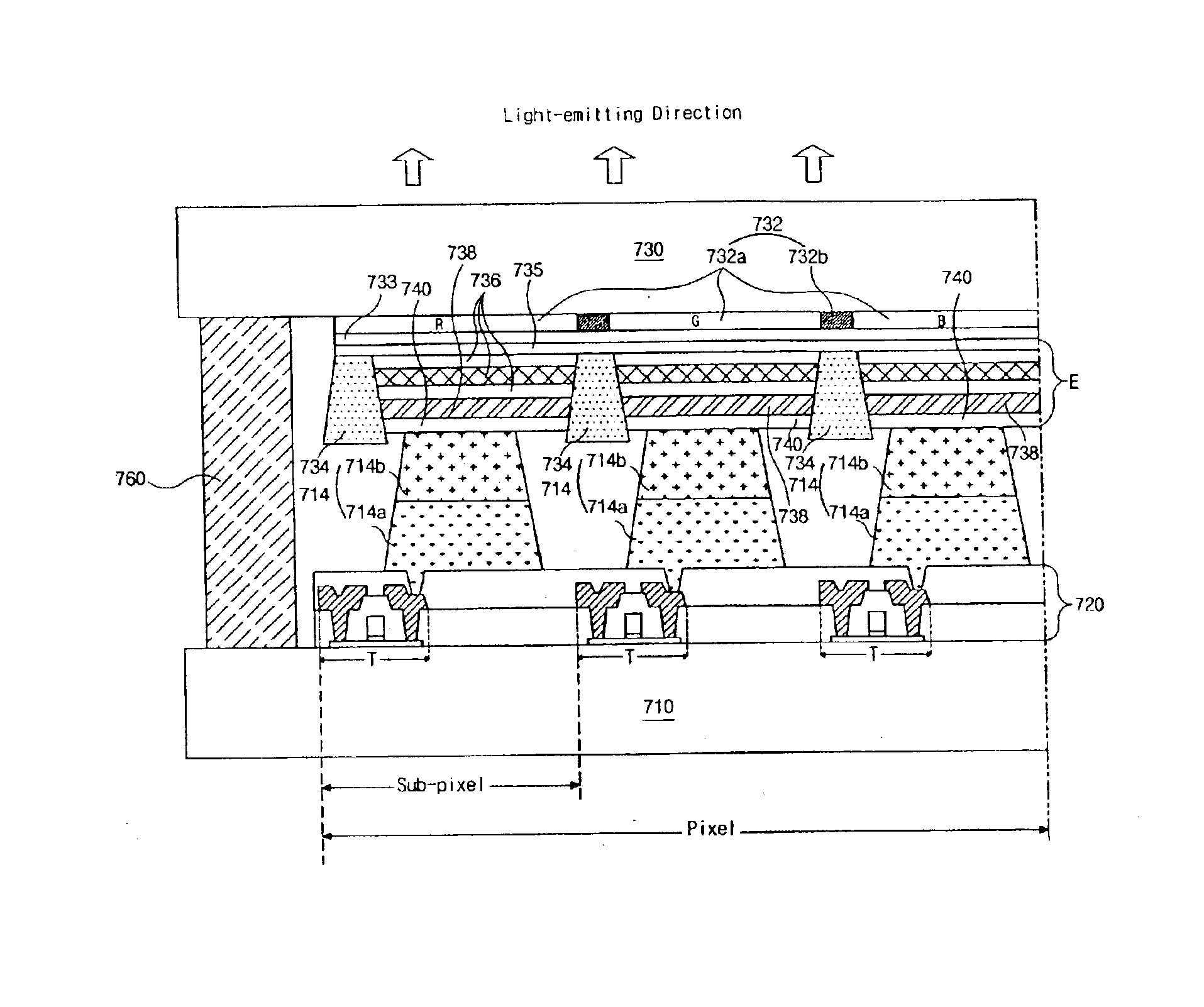
FIG. 5 is a cross-sectional view of a top emission type organic electroluminescent display device showing one pixel according to the present invention. As shown in FIG. 5, first and second substrates 110 and 130 are spaced apart from each other. The first and second substrates 110 and 130 are attached to each other by a seal pattern 140. On a front surface of the first substrate 110, array elements 120 are formed. On a rear surface of the second substrate 130, organic electroluminescent diodes E are disposed. Each of the organic electroluminescent diodes E includes a first electrode 132, electrode separator 134, an organic electroluminescent layer 136 and a second electrode 138. The first electrode 132 is disposed on the whole surface of the second substrate 130 and acts as a common electrode. The electrode separators 134 are formed of an insulating material. Electrode separators 134 are disposed inboard of a pixel such that the electrode separators 134 divide a pixel into three sub...

fourth embodiment

FIG. 10 is an enlarged cross-sectional view illustrating a thin film transistor and conductive connector according to the present invention. As shown, a semiconductor layer 350 of polycrystalline silicon and a capacitor electrode 352 are formed on the first substrate 310. On the central part of the semiconductor layer 350, a gate insulation layer 354 and the gate electrode 356 are sequentially formed. An interlayer insulator 358 is formed on the first substrate 310 to cover the semiconductor layer 350, the capacitor electrode 352 and the gate electrode 356. The interlayer insulator 358 has first and second contact holes 360 and 362 that expose portions of the semiconductor layer 350, respectively, on both sides of the gate electrode 356. Source and drain electrodes 364 and 366 are formed on the interlayer insulator 358, and contact the semiconductor layer 350 through the first contact hole 360 and through the second contact hole 362, respectively. A power electrode 368 is formed on ...

fifth embodiment

In the present invention, a buffer electrode 440 is formed on the rear surface of each of the organic electroluminescent diodes E. Thus, a plurality of conductive connectors 414 is disposed between the array elements 420 of the first substrate 410 and the buffer electrode 440. More specifically, each of the organic electroluminescent diodes E further includes a buffer electrode 440 on the rear surface of the second electrode 438. Since the buffer electrode 440 is formed of a conductive material, the conductive connectors 414 electrically connect the thin film transistors T to the organic electroluminescent diode E.

The first and second electrodes 432 and 438 of the organic electroluminescent diode E are generally formed in an evaporator. However, the metal thin films of the first and second electrodes 432 and 438, which are formed in an evaporator, are easily damaged and separate easily from the organic electroluminescent diode E. The buffer electrode 440 formed on the second electro...


PUM


Abstract

An organic electroluminescent device includes first and second substrates attached by a seal pattern, array elements including a plurality of thin film transistors formed on the first substrate, a first electrode formed on a rear surface of the second substrate, a plurality of electrode separators formed on the rear surface of the first electrode, wherein the plurality of electrode separators is made of an insulating material defining sub-pixel regions that correspond to each thin film transistor, an organic electroluminescent layer formed on a rear surface of the first electrode in each of the sub-pixel regions, a second electrode formed on a rear surface of the organic electroluminescent layer in each of sub-pixel regions, a conductive connector formed between the first and second substrates in each sub-pixel region for connecting to the second electrode of a sub-pixel region.

Description

The present application claims the benefit of Korean Patent Application No. 2002-22812 filed in Korea on Apr. 25, 2002, which is hereby incorporated by reference in its entirety.BACKGROUND OF THE INVENTION1. Field of the InventionThe present invention relates to organic electroluminescent devices, and more particularly, to a top emission type active matrix organic electroluminescent device.2. Discussion of the Related ArtFlat panel display devices—which are characterized as being thin, light weight and energy efficient—are in high demand in the display field as the information age rapidly evolves. A flat panel display device can be classified into one of two types depending on whether it emits or receives light. One type is a light-emitting type display device that emits light to display images, and the other type is a light-receiving type display device that uses an external light source to display images. Plasma display panels, field emission display devices, and electroluminescen...

Claims


Application Information

Patent Timeline
Patent Type & Authority Patents(United States)
IPC IPC(8): H01L27/32H01L27/28H01L51/52H01L51/50G09F9/30H05B33/26
CPCH01L27/3253H01L27/3211H01L27/322H01L27/3246H01L2251/5315H01L27/3295H01L51/5237H10K59/35H10K59/38H10K59/1275H10K59/122H10K50/841H10K2102/3026H05B33/26
Inventor PARK, JAE YONGKIM, OCK HEEYOO, CHOONG KEUNLEE, NAM YANGKIM, KWAN SOO
Owner LG DISPLAY CO LTD
Why Eureka
Try Eureka