Power semiconductor device

a technology of power semiconductor and semiconductor device, which is applied in the direction of transistors, basic electric elements, substation/switching arrangement casings, etc., can solve the problems of increasing the overall packaging area, malfunction or breakdown of the power conversion device, etc., and achieve the effect of reducing the wiring inductance and packaging area

Active Publication Date: 2005-03-22
MITSUBISHI ELECTRIC CORP
View PDF3 Cites 23 Cited by
  • Summary
  • Abstract
  • Description
  • Claims
  • Application Information

AI Technical Summary

Benefits of technology

[0011]The number of the bus electrodes becomes fewer and the bus bar correspondingly gets shorter. Therefore, the wiring length thereby shortened allows a reduction of the wiring inductance. Moreover, since the bus bar is arranged between the elements, a packaging area can be reduced.
[0013]The insulating property may be enhanced by sealing the first to fourth resin-sealed switching elements and the bus bar together.

Problems solved by technology

A power conversion device, typically a conventional inverter or converter having the 1 in 1 type power module and a control circuit thereof within, has presented the following problem: namely, a semiconductor substrate and the like included in the control circuit is subjected to strong noise and electromagnetic waves generated by a wiring inductance at the time of switching of the switching element, resulting in a malfunction or a breakdown of the power conversion device.
Another problem with the conventional power conversion device is an increase in the overall packaging area because of a wiring bus bar mounted outside the sealing resin.
Those are thus less-than-optimal structures when they are premised on the use of the 1 in 1 type power module, leaving problems from the viewpoints of wiring inductance, packaging area and the like.

Method used


Image

  • Power semiconductor device
  • Power semiconductor device
  • Power semiconductor device

Examples


Embodiment Construction

ferred embodiment;

[0022]FIG. 8 shows a structure of an element used in a power conversion device 3 according to a third preferred embodiment of the invention;

[0023]FIG. 9 shows a structure of an element used in the power conversion device 3 according to the third preferred embodiment; and

[0024]FIG. 10 is a perspective view showing a connection configuration of the elements in the power conversion device 3 according to the third preferred embodiment.

DESCRIPTION OF THE PREFERRED EMBODIMENTS

[0025]

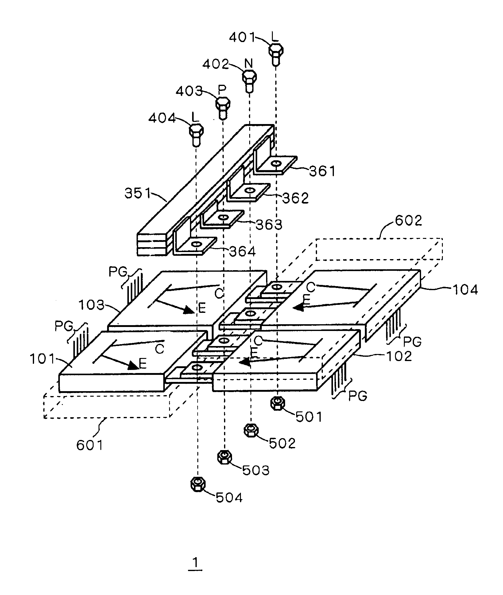
[0026]A power semiconductor device (power conversion device) according to a first preferred embodiment of the present invention features a reduction in length of a bus bar and packaging area, by arranging two power module elements each on both sides of the bus bar rather than arranging four power module elements on one side of the bus bar. Namely, the elements arranged in twos face each other with the bus bar between.

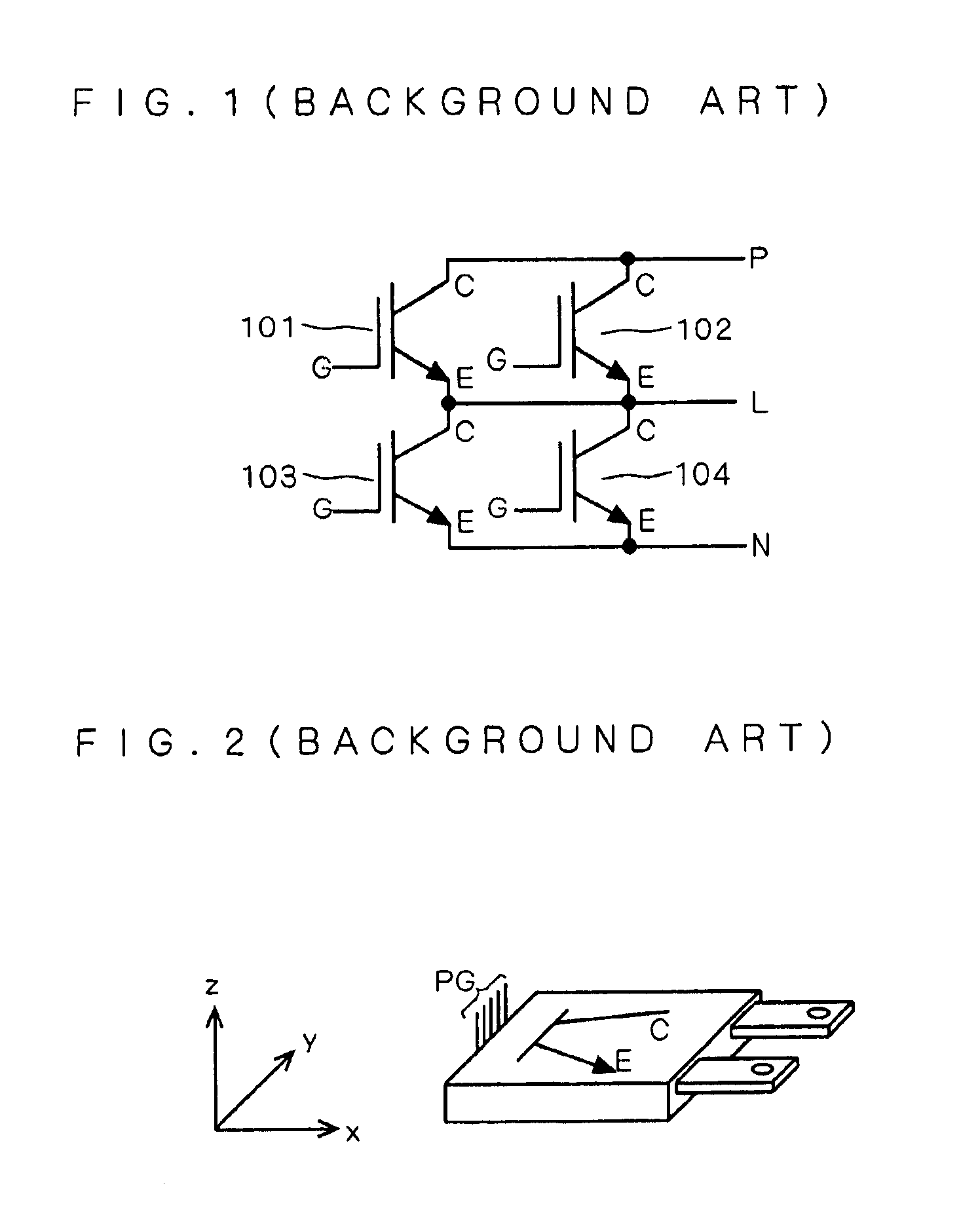
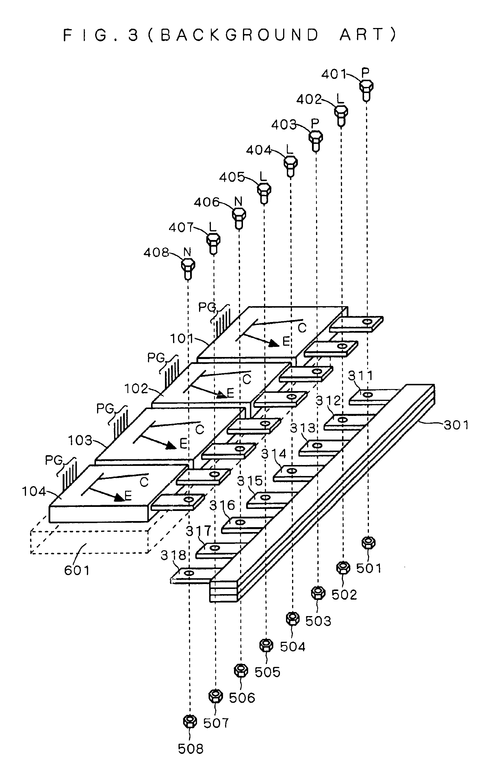
[0027]First, as a background to the present preferred embodiment, a configura...


PUM


Abstract

Emitter electrodes (Es) and collector electrodes (Cs) of elements (101 to 104) are connected to bus electrodes (361 to 364) of a bus bar (351), respectively. The bus bar (351) contains seven layers including four insulating layers (not shown) and three conductive layers (shown) interposed between the insulating layers. Namely, each of the bus electrodes (361 to 364) is connected to one of the conductive layers corresponding to one of a positive electrode (P), a negative electrode (N) and an intermediate electrode (L). The collector electrodes (Cs) of the elements (103 and 104) are connected one over the other to the bus electrode (361). The emitter electrodes (Es) of the elements (103 and 104) are connected one over the other to the bus electrode (362). The collector electrodes (Cs) of the elements (101 and 102) are connected one over the other to the bus electrode (363). The emitter electrodes (Es) of the elements (101 and 102) are connected one over the other to the bus electrode (364).

Description

BACKGROUND OF THE INVENTION[0002]1. Field of the Invention[0003]The present invention relates to a power semiconductor device, and more particularly to a technique of connecting switching elements in parallel which are sealed with resin by the transfer mold process and the like in a power control device and the like.[0004]2. Description of the Background Art[0005]In general, a power semiconductor element including one switching element (a MOS-FET, a bipolar transistor, an IGBT and the like) which is sealed with resin by the transfer mold process and the like is termed a 1 in 1 type power module. A power conversion device, typically a conventional inverter or converter having the 1 in 1 type power module and a control circuit thereof within, has presented the following problem: namely, a semiconductor substrate and the like included in the control circuit is subjected to strong noise and electromagnetic waves generated by a wiring inductance at the time of switching of the switching ...

Claims


Application Information

Patent Timeline
Patent Type & Authority Patents(United States)
IPC IPC(8): H01L25/11H01L25/10H01L25/07H01L25/18
CPCH01L25/115H01L2924/0002H01L2924/00
Inventor USHIJIMA, KOICHI
Owner MITSUBISHI ELECTRIC CORP
Why Eureka
Try Eureka