Multilayer wiring board

a wiring board and multi-layer technology, applied in the direction of printed circuit details, printed circuit aspects, printed circuit manufacturing, etc., can solve the problems of disturbance of the increase in speed, the pitch difference between the terminals on the ic chip and the mother board side, and the difficulty of directly connecting the ic chip onto the mother board, so as to increase the adhesion strength and enhance the product yield

Inactive Publication Date: 2009-09-17
NGK SPARK PLUG CO LTD
View PDF6 Cites 34 Cited by
  • Summary
  • Abstract
  • Description
  • Claims
  • Application Information

AI Technical Summary

Benefits of technology

[0009]Exemplary embodiments of the present invention provide a multilayer wiring ...

Problems solved by technology

However, a great difference is made in a pitch between the terminals on the IC chip and the mother board side.
Therefore, it is hard to directly connect the IC chip onto the mother board.
In this case, the wiring penetrating the core board contributes as a high inductance so that a transmission loss of a radio frequency signal or a circuit malfunction is caused, resulting in a disturbance of the increase in the speed.
Since the coreless wiring ...

Method used


Image

  • Multilayer wiring board
  • Multilayer wiring board
  • Multilayer wiring board

Examples


Embodiment Construction

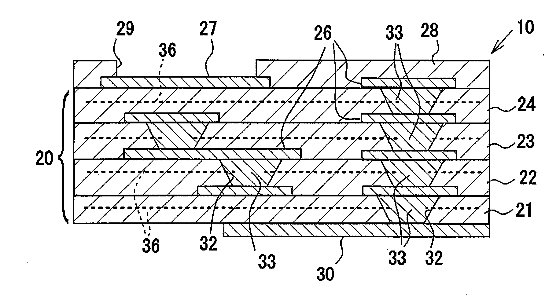
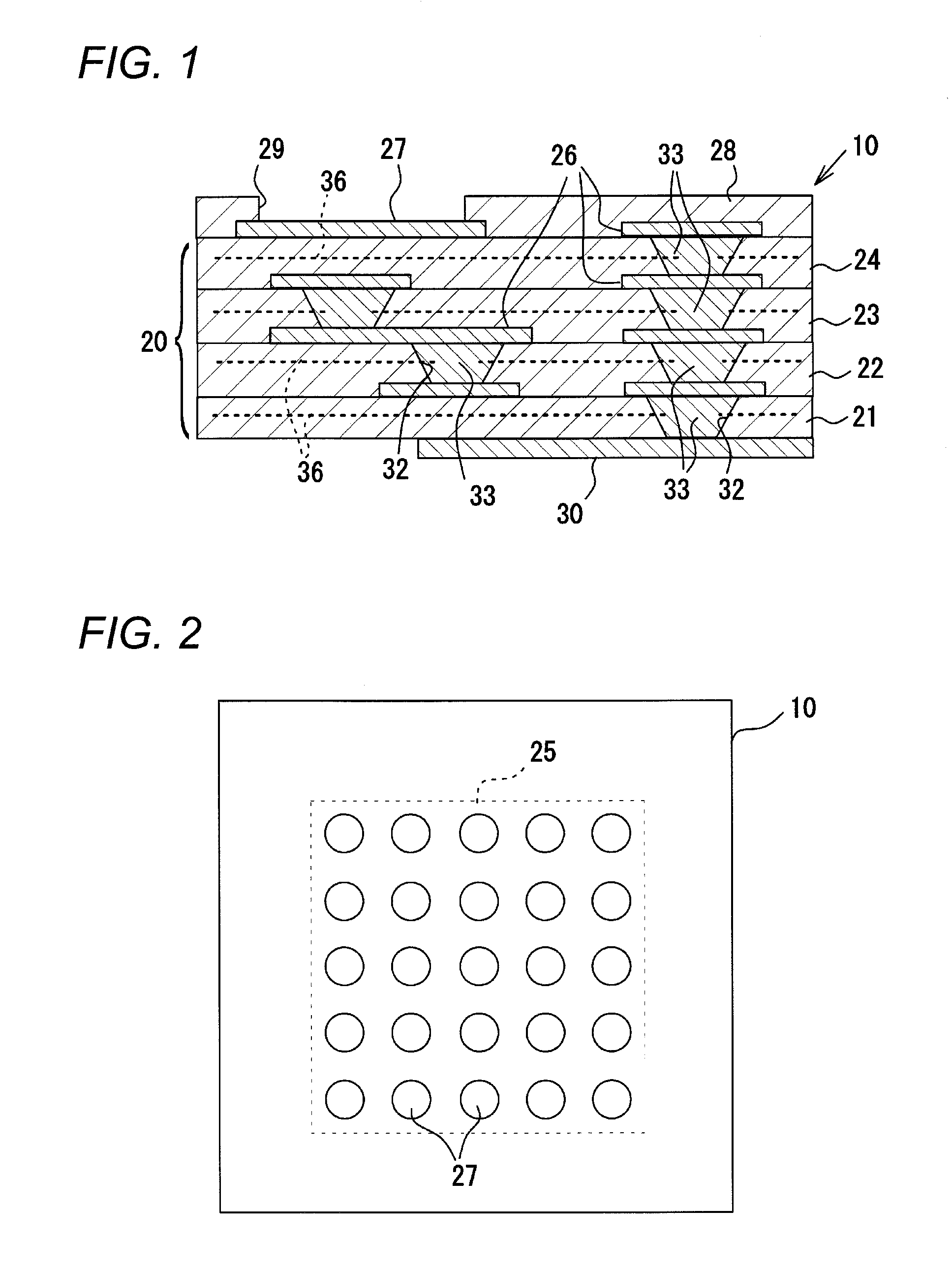
[0042]An embodiment according to the invention will be described below in detail with reference to the drawings. FIG. 1 is an enlarged sectional view showing a schematic structure of a coreless wiring board (a multilayer wiring board) according to the embodiment and FIG. 2 is a plan view showing the coreless wiring board.

[0043]As shown in FIG. 1, a coreless wiring board 10 has no core board but a wiring laminated portion 20 (a laminated structure) in which four resin insulating layers (insulating layers) 21, 22, 23 and 24 formed of an epoxy resin and a conductor layer 26 formed of copper are alternately laminated into a multilayer. In the coreless wiring board 10, a terminal pad 27 is provided on a surface (an upper surface) of the resin insulating layer 24 to be the fourth layer. FIG. 1 is a sectional view showing a part of the coreless wiring board 10. A plurality of terminal pads 27 is disposed in an array on an upper surface of the coreless wiring board 10, for example (see FIG....


PUM

PropertyMeasurementUnit
Angleaaaaaaaaaa
Depthaaaaaaaaaa
Processing propertiesaaaaaaaaaa

Abstract

A coreless wiring board has no core board but a laminated structure in which a conductor layer and resin insulating layers are alternately laminated into a multilayer. Each of the resin insulating layers is formed to contain a glass cloth in an epoxy resin. A plurality of via holes taking a shape of an inverse truncated cone and having steps on internal wall surfaces is formed to penetrate each of the resin insulating layers, and a filled via conductor for electrically connecting the conductors is formed in each of the via holes.

Description

CROSS-REFERENCE TO RELATED APPLICATIONS[0001]This application is based upon and claims priority from Japanese Patent Application No. 2008-064987 filed on Mar. 13, 2008, the entire contents of which are incorporated herein by reference.BACKGROUND OF THE INVENTION[0002]1. Field of the Invention[0003]The present disclosure relates to a multilayer wiring board having no core board but a laminated structure in which a conductor layer and an insulating layer are alternately laminated into a multilayer.[0004]2. Description of Related Art[0005]In recent years, a semiconductor integrated circuit device (an IC chip) to be used as a microprocessor of a computer has increasingly been enhanced in a speed and a function, and incidentally, there is a tendency that the number of terminals is increased and a pitch between the terminals is also reduced. In general, a large number of terminals are densely disposed in an array on a bottom face of the IC chip, and the terminal group is connected to that...

Claims


Application Information

Patent Timeline
IPC IPC(8): H05K1/11
CPCH05K1/0366H05K3/0035H05K3/007H05K2203/0152H05K3/4682H05K2201/09563H05K2201/09845H05K3/421
Inventor KATAGIRI, HIROSHIASANO, TOSHIYA
Owner NGK SPARK PLUG CO LTD
Why Eureka
Try Eureka