Low voltage differential in differential out receiver

a receiver and low voltage technology, applied in the field of interface circuits, can solve the problems of increasing jitter and limiting the practical circuit to higher vcc levels, and achieve the effects of improving low vcc performance, reducing output voltage, and reducing skew and jitter

Inactive Publication Date: 2005-03-22
SEMICON COMPONENTS IND LLC
View PDF9 Cites 15 Cited by
  • Summary
  • Abstract
  • Description
  • Claims
  • Application Information

AI Technical Summary

Benefits of technology

In view of the foregoing background discussion, the present invention provides a high speed, low voltage, low power, differential receiver that provides lower skew and jitter over a wide range of common mode input signal levels. The present invention also provides a lower output voltage swing from the second stage that improves the low Vcc performance of the invention.
The present invention includes a folded cascode made up of a differential input stage and a load or current summation stage, and a second differential stage. The differential input stage includes first NMOS pair and a PMOS pair of differentially connected transistors that accept a rail to rail input common mode signal level. The load or summation stage follows with a full ground to Vcc output signal only at thesecond differential stage. This arrangement provides a lower gain second stage with a lower output voltage swing, lower power dissipation, better crossover control, high speed, and better jitter and skew performance.
The differential input and load or current summation stages share current sources, and the differential signal is transferred between these stages via these shared current sources. The better performance is due partly to keeping the current sources substantially constant over a wider range of common mode input voltage levels. The reduced signal voltage swings of the load or summation stage allows the current sources to remain operational over a wider range of input common signal levels and at lower Vcc levels than if the output of that stage traversed from ground to Vcc. The reduced load or summation stage output voltage swing also benefits by keeping impedances and cross over points relatively constant over wider ranges of common mode signal levels. The second differential stage does not share currents and is relatively unaffected by the input common mode signal level. This stage provides a differential output signal with higher voltage drive for complementary CMOS inverters that provide a differential output signal, but with the higher currents available this stage performs at high frequencies and its input differential switching threshold remains substantially constant and does not appreciably affect the crossover point.

Problems solved by technology

Moreover, the combined effect of input signal common mode level on the second stage, and second stage wide dynamic output range, limits practical circuits to higher Vcc levels.
This crossover point change increases jitter.

Method used


Image

  • Low voltage differential in differential out receiver
  • Low voltage differential in differential out receiver
  • Low voltage differential in differential out receiver

Examples


Embodiment Construction

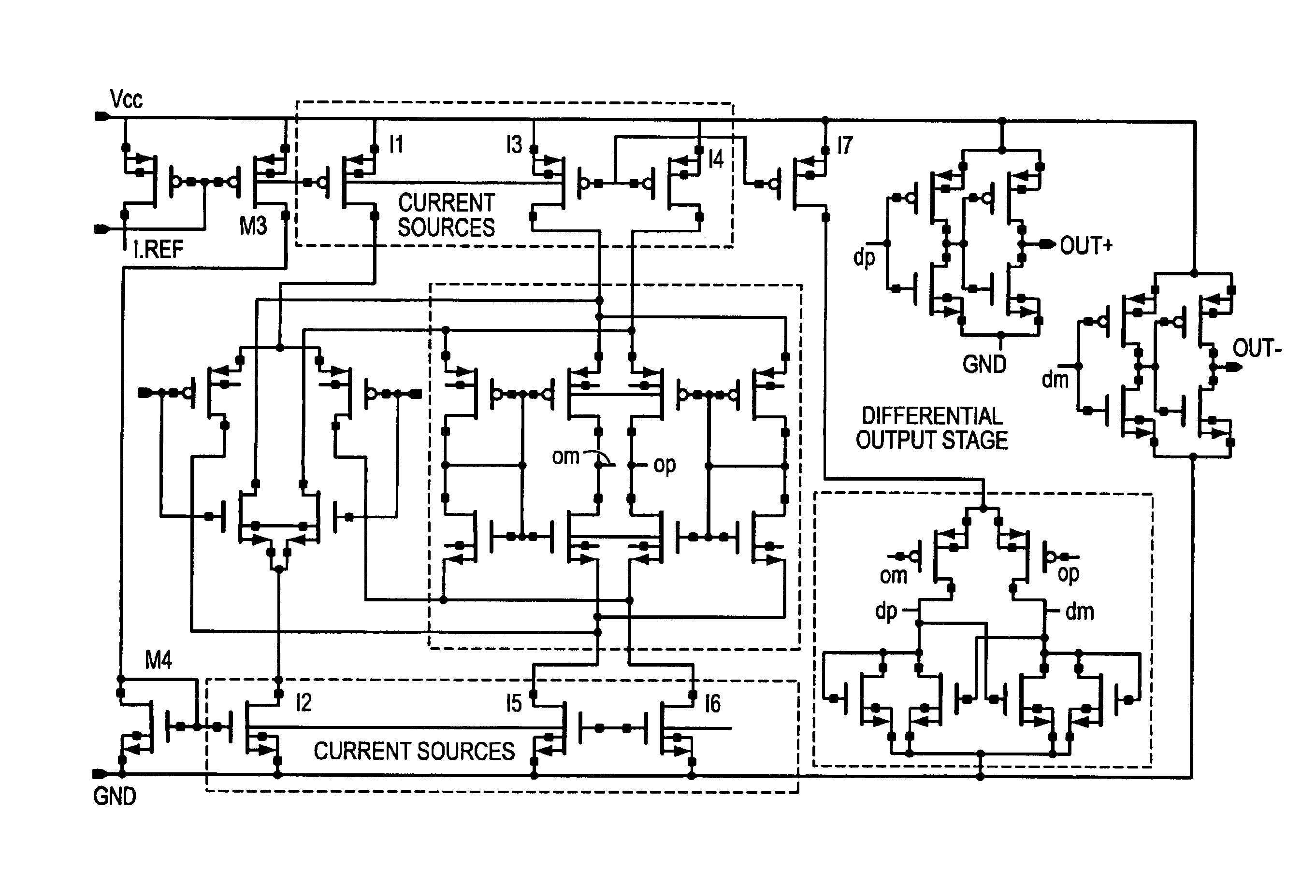
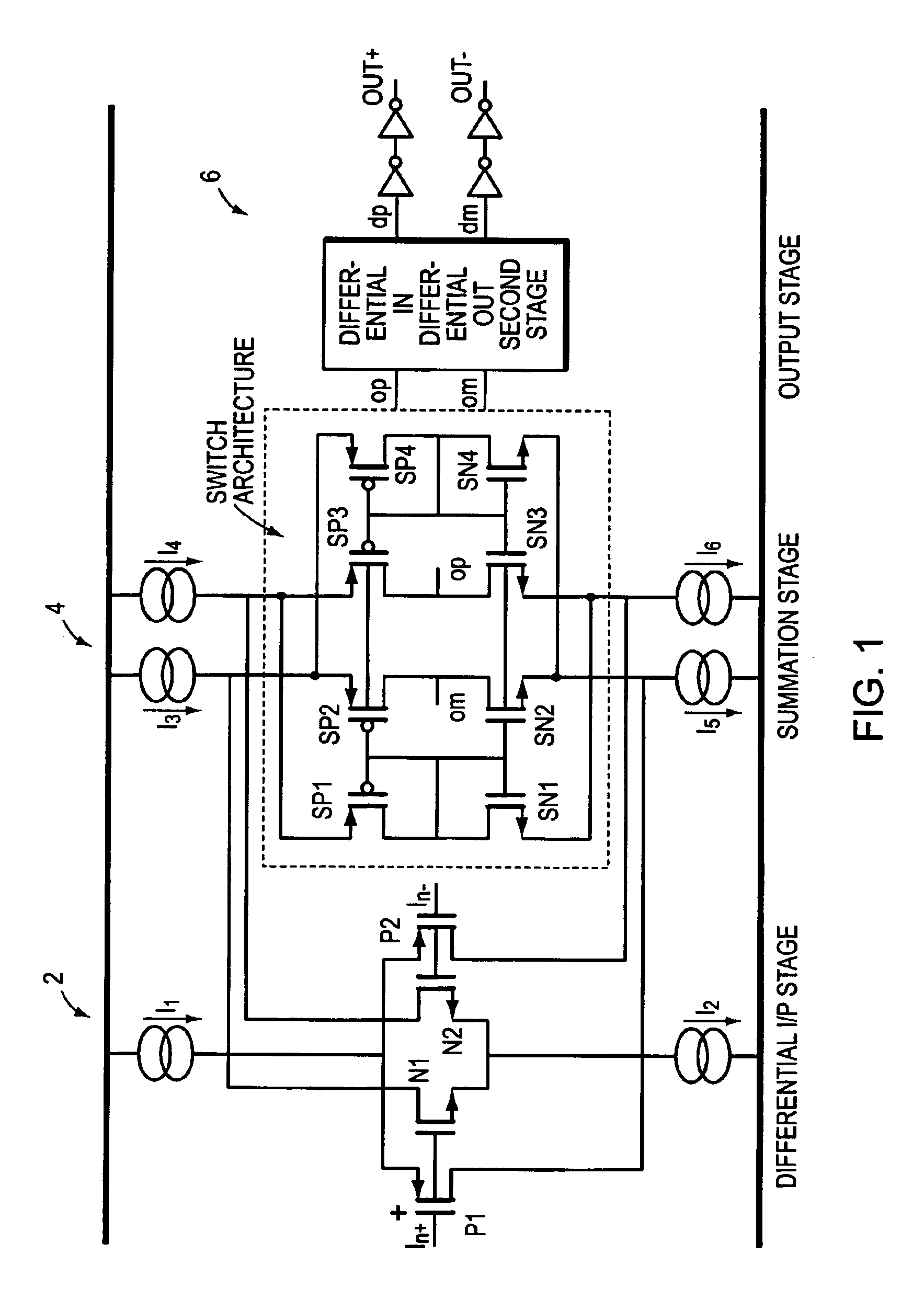
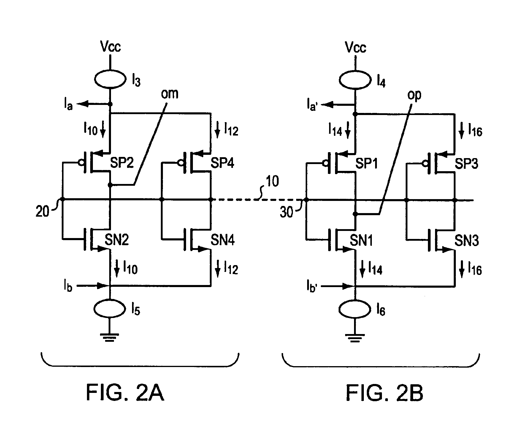
. 1 is a schematic block diagram of a folded cascode 2 comprised of source coupled NMOS transistors, N1 and N2, with a current source I2 connecting the sources to ground. There is a parallel set of PMOS transistors, P1 and P2, sharing a current source I1 connecting their sources to the power rail, Vcc. I1 and I2 are complementary current sources, typically of equal value. The value may range widely from microamps to milliamps or more depending on applications. In one preferred embodiment I1 and I2 are arranged to provide 0.350 milliamps. The gates of N1 and P1 are connected together and to an input signal, In+, and the gates of N2 and P2 are similarly connected together and to the complementary input signal, In−. Each of the drains of the input stage NMOS and PMOS transistors are connected together, in a folded cascode fashion, to sources of opposite polarity transistors in the load or current summation stage 4. Folded cascode circuits have the beneficial characteristic of a differe...


PUM


Abstract

A folded common cascode circuit with symmetric parallel signal paths from the differential inputs to a single ended output provides a low skew, low jitter, low power, high speed differential in/out amplifier. There is a differential input stage followed by a load or current summation stage with all gates tied together, and then a second differential stage. The dynamic voltage range of the second stage allows for lower Vcc operation while providing improved jitter operation. The signal paths on either side of the differential amplifier are made equal with equal loads along each path. Pairs of complementary NMOS and PMOS transistor pairs with parallel complementary biasing current mirroring stacks on the cascode circuitry have all their gates connected together. The layout maintains symmetrical parallel signal paths and symmetrical amplification and impedance loading from differential input to the differential output. Output inverters provide a higher drive capability.

Description

BACKGROUND OF THE INVENTION1. Field of the InventionThe present invention relates to interface circuits, and more particularly to Input / Output (I / O) circuits and receivers, and even more particularly to high speed, low voltage, low power, differential input, low jitter and skew I / O receiver circuits that provide a differential output (LVDO).2. Background InformationLow voltage differential signals are common for high-speed signal transmission. Saturation effects are avoided and power dissipation is limited, and, since low voltage signals are prone to noise, use of differential signals, where the noise is common to both signals, generally overcomes this problem.However, since common mode signals will occur, LVDO circuits are designed to accept differential signals that ride on a common mode level that may range from the low power (ground) rail to the Vcc power rail.U.S. Pat. Nos. 5,801,564; 6,252,432 B1 and 6,236,269 B1 set out a high speed circuits that operate over a wide input com...

Claims


Application Information

Patent Timeline
Patent Type & Authority Patents(United States)
IPC IPC(8): H03F3/45
CPCH03F3/45219H03F3/45192
Inventor PRADHAN, PRAVASCHITNIS, SHAILESH
Owner SEMICON COMPONENTS IND LLC
Why Eureka
Try Eureka