Method for fabricating a lithographic reflection mask in particular for the patterning of a semiconductor wafer, and a reflection mask

a technology of lithographic reflection and reflection mask, which is applied in the field of lithographic reflection mask fabrication, to achieve the effect of reducing radiation losses, minimizing mechanical stresses in the reflection mask, and reducing radiation losses at the sidewalls

Inactive Publication Date: 2005-03-29
POLARIS INNOVATIONS LTD
View PDF3 Cites 15 Cited by
  • Summary
  • Abstract
  • Description
  • Claims
  • Application Information

AI Technical Summary

Benefits of technology

The method according to the invention for fabricating a lithographic reflection mask, in particular for extremely small feature sizes below 100 nm, has the constructive advantage that the absorber layer is applied on the top side of the substrate below the reflection layer and / or on the side areas of the reflection layer. The above-mentioned disadvantages such as the undesired shadowing effects are largely avoided by virtue of the changed configuration of the reflection layer and the absorber layer, since now the patterned reflection layer can be projected onto the wafer in an undisturbed and image-faithful manner. The absorber layer produces no shadowing effects, or only greatly reduced shadowing effects, on account of the special configuration below the reflection layer and / or on the sidewalls of the reflection layer. In this case, what is regarded as particularly advantageous is that, moreover, no asymmetrical or significantly fewer asymmetrical intensity profiles of the reflected radiation arise, so that it is practically impossible for undesired asymmetrical resist structures to occur on the wafer. The reflection mask constructed in this way supports a stable projection process that, in production engineering use, advantageously ensures a high reliability during the patterning of the wafer.
The reflection mask is preferably used for the EUV lithography of a semiconductor wafer, the EUV radiation lying in the range from 10 to 15 nm. The wavelength makes it possible to produce extremely small structures far below 100 nm.

Problems solved by technology

This is not provided in the known fabrication methods for reflection masks, where defects or particles act as solid faults since generally they cannot be removed without damage to the reflector layer.

Method used


Image

  • Method for fabricating a lithographic reflection mask in particular for the patterning of a semiconductor wafer, and a reflection mask
  • Method for fabricating a lithographic reflection mask in particular for the patterning of a semiconductor wafer, and a reflection mask
  • Method for fabricating a lithographic reflection mask in particular for the patterning of a semiconductor wafer, and a reflection mask

Examples


Embodiment Construction

In order to provide a better understanding of the invention, the known prior art with its problems will be explained in more detail. The miniaturization of structures which are intended to be produced in a dimension of from 70 to 35 nm requires lithographic reflection masks which can be used with a wavelength in the soft X-ray range from 10 to 15 nm.

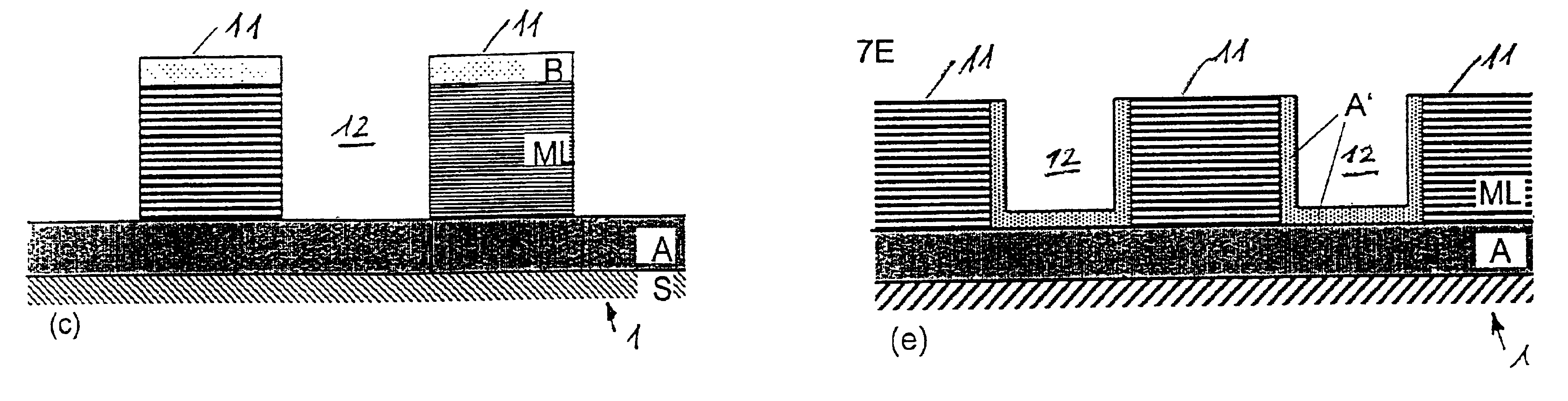
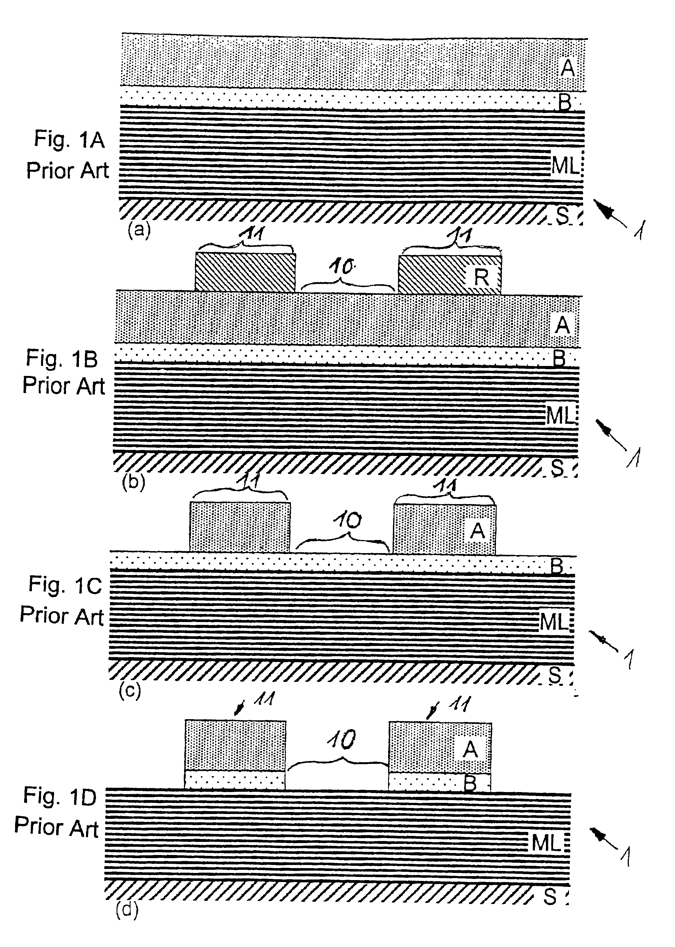
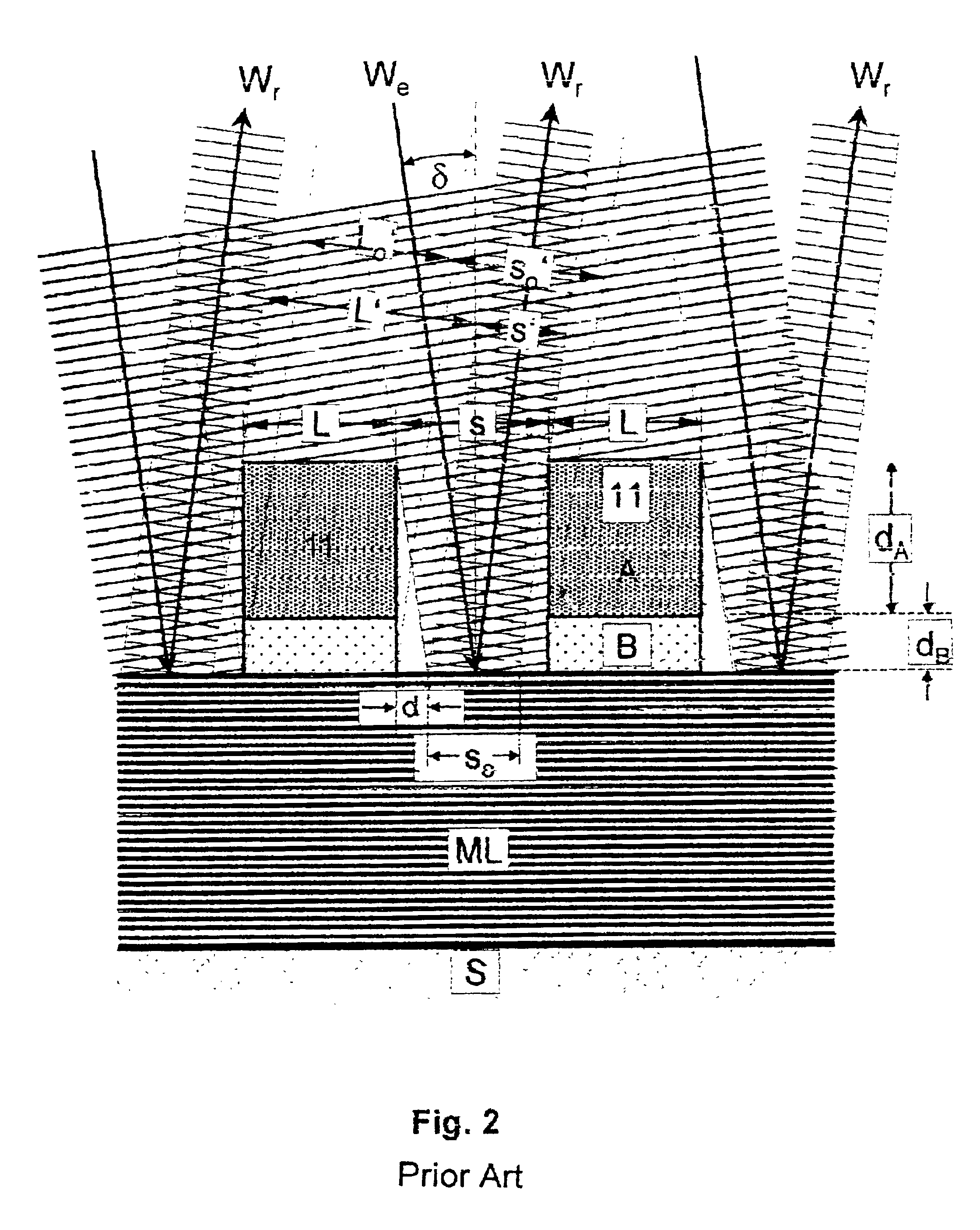
Referring now to the figures of the drawing in detail and first, particularly, to FIGS. 1A to 1D thereof, there is shown, in a sectional view, a diagrammatic construction of a reflection mask 1, which can be created by an absorber etching process, for example. In this case, in accordance with FIG. 1A, a starting point is a substrate S composed, for example, of a quartz glass or ultra-low-expansion (ULE) material. A reflection layer ML, formed as a multilayer layer, is applied to the substrate S. The multilayer layer ML is formed with a multiplicity of thin layers, the layer thickness of an individual layer corresponding approximately to ...


PUM

PropertyMeasurementUnit
thicknessaaaaaaaaaa
thicknessaaaaaaaaaa
total thicknessaaaaaaaaaa

Abstract

A method for fabricating a lithographic reflection mask in particular for patterning of semiconductor wafers, is described, and can be used for extremely small feature sizes below 100 nm. In known lithographic methods with EUV radiation (extreme ultraviolet), for the mask fabrication, a multilayer reflection layer is applied to a substrate. An absorber layer is deposited after the multilayer layer is patterned above the multilayer layer or is completely introduced into the latter. In the case of the method according to the invention, in contrast, the absorber layer is applied between the substrate and the reflection layer and / or on the side areas of the reflection layer. This has the advantage of reducing CD changes due to shadowing of structures lying above the reflection layer. Further advantages are, inter alia, smaller structure displacements and reduced asymmetrical intensity profiles of the reflected beams of radiation.

Description

BACKGROUND OF THE INVENTIONField of the InventionThe invention is based on a method for fabricating a lithographic reflection mask, in particular for feature sizes below 100 nm. For the fabrication in particular of semiconductor chips on a silicon wafer (wafer), it is already known to use reflection masks that contain the structures that are projected onto the wafer. In order to optimize and reduce fabrication costs, the semiconductor industry endeavors to make the feature sizes on the semiconductor chips as small as possible. The miniaturization of the structures allows more transistor functions to be realized in an extremely small space.Known optical lithography methods enable feature sizes of approximately 100 nm to be controlled in terms of production engineering. However, goals for the next few years are for the feature sizes to be considerably reduced; by way of example, line widths of 35-70 nm are sought for extremely small structures. Known optical lithography methods, in wh...

Claims


Application Information

Patent Timeline
Patent Type & Authority Patents(United States)
IPC IPC(8): G03F1/14G03F1/08G03F1/00G03F1/22G03F1/24
CPCB82Y10/00B82Y40/00G03F1/24G03F1/22G03F1/08
Inventor SCHWARZL, SIEGFRIED
Owner POLARIS INNOVATIONS LTD
Why Eureka
Try Eureka