Group III nitride compound semiconductor device

Inactive Publication Date: 2005-03-29
TOYODA GOSEI CO LTD
View PDF17 Cites 8 Cited by
  • Summary
  • Abstract
  • Description
  • Claims
  • Application Information

AI Technical Summary

Benefits of technology

[0019]An object of the present invention is to form a group III nitride compound semiconductor layer, especially, a GaN semiconductor layer, of a good crystal structure by using industrially available raw materials. As a result, a semiconductor device according to the present invention can be provided with a semiconductor layer of a good crystal structure and produced inexpensively.
[0029]In the semiconductor light-emitting device configured as described above according to the present invention, a GaN light-emitting layer is formed on the undercoat layer of metal nitride formed on the substrate. The GaN light-emitting layer of a good crystal can be grown on the undercoat layer because the lattice mismatch between the undercoat layer and the light-emitting layer formed on the undercoat layer can be reduced by adjustment of the composition of metal nitride. On the other hand, the thickness of the undercoat layer can be reduced because the substrate can have a thickness required for holding the function of the device. Hence, the undercoat layer can be formed easily and inexpensively. If a general substrate such as a sapphire substrate is used as the substrate, the device can be produced inexpensively as a whole.
[0030]Moreover, in the configuration of the present invention, a reflection layer of metal nitride may be provided just under the light-emitting layer. Light emitted from the light-emitting layer toward the substrate is reflected by the reflection layer because the reflection layer has a gloss of metallic color so that the reflection layer reflects visible light. Further, the substantial whole of the light toward the substrate is reflected by the reflection layer because the reflection layer is disposed just under the light-emitting layer. As a result, the substantial whole of the light emitted from the light-emitting layer toward the substrate can be utilized effectively, so that improvement of the brightness of the light-emitting device can be attained.

Problems solved by technology

Metal nitride having such a thickness, however, has not been provided as a raw material of an industrial product used for production of a semiconductor.
Hence, light emitted from the light-emitting device cannot be used effectively.
Moreover, the sapphire substrate is expensive.
Further, because n-type and p-type electrodes are formed on one face side, reduction of the device size is limited.
In addition, there is a “charge-up” problem.
According to the inventors' examination, it was, however, very difficult to grow a GaN semiconductor layer on the Si substrate.
On cause of the difficulty is the difference in thermal expansibility between Si and the GaN semiconductor.
On this occasion, tensile stress is generated in the GaN semiconductor layer, so that there is a risk of occurrence of cracking as a result.
Hence, the GaN semiconductor device cannot fulfill its original function.
As a result, the distance of the electricity path increases and resistance is increased unavoidably.
As a result, the operating voltage of the device becomes high.
There is also a problem that withstand electrostatic stress characteristic is worsened because of the current concentration.
Hence, there is a further problem that the permissible current cannot be set to be large.

Method used


Image

  • Group III nitride compound semiconductor device
  • Group III nitride compound semiconductor device
  • Group III nitride compound semiconductor device

Examples


third embodiment

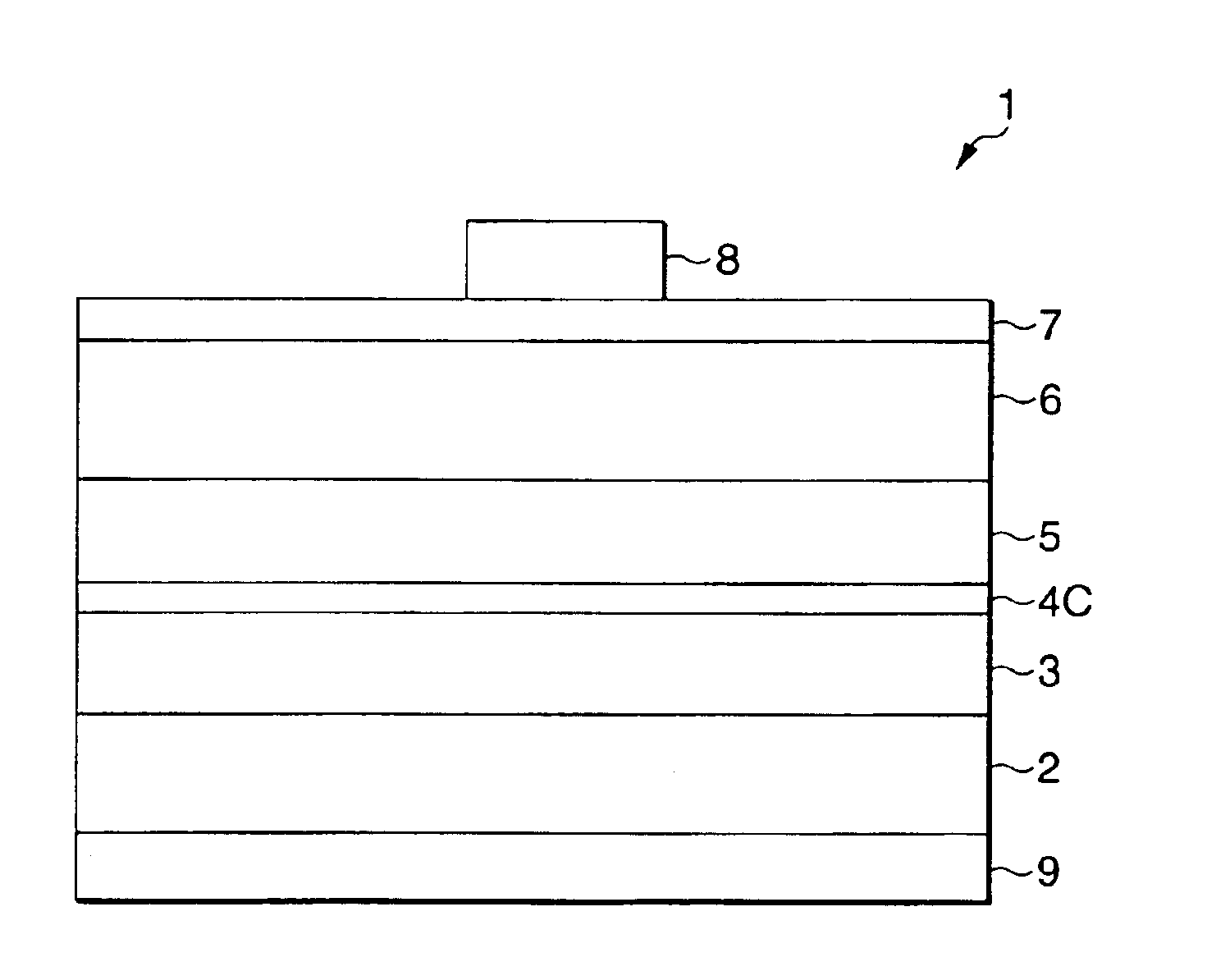
[0043]FIG. 11 is a view showing the configuration of a light-emitting diode as the present invention;

fourth embodiment

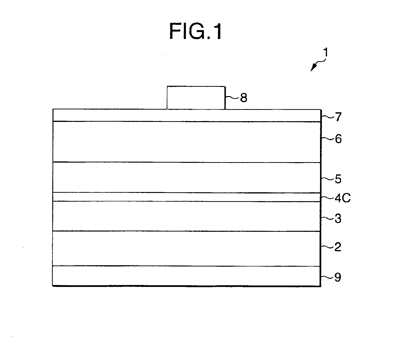
[0044]FIG. 12 is a view showing the configuration of a light-emitting diode as the present invention;

[0045]FIG. 13 shows a result of φ(PHI) scanning of a sample 3;

[0046]FIG. 14 shows a result of φ(PHI) scanning of a sample 4;

[0047]FIG. 15 shows a result of φ(PHI) scanning of a sample 5;

[0048]FIG. 16 shows a result of φ(PHI) scanning of a sample 6;

[0049]FIG. 17 shows a result of φ(PHI) scanning of a sample 8;

[0050]FIG. 18 shows a result of φ(PHI) scanning of a sample 9;

[0051]FIG. 19 shows a result of φ(PHI) scanning of a sample 13;

[0052]FIG. 20 shows a result of φ(PHI) scanning of a sample 14;

[0053]FIG. 21 shows a result of φ(PHI) scanning of a sample 15;

[0054]FIG. 22 shows a result of φ(PHI) scanning of a sample 16;

fifth embodiment

[0055]FIG. 23 shows the configuration of a light-emitting diode as a fifth embodiment;


PUM


Abstract

An undercoat layer inclusive of a metal nitride layer is formed on a substrate. Group III nitride compound semiconductor layers are formed on the undercoat layer continuously.

Description

[0002]This is a Divisional of U.S. application Ser. No. 09 / 518,724, filed Mar. 3, 2000 now U.S. Pat. No. 6,426,512 the entire contents of which are incorporated by reference.BACKGROUND OF THE INVENTION[0003]1. Field of the Invention[0004]This invention relates to a group III nitride compound semiconductor device. More particularly, it relates to an improvement in an undercoat layer for a group III nitride compound semiconductor layer such as a GaN semiconductor layer.[0005]The present application is based on Japanese Patent Applications No. Hei. 11-58128, 11-60206, 11-611155, 11-90833, and 11-235450, which are incorporated herein by reference.[0006]2. Description of the Related Art[0007]The fact that a (111) face of metal nitride exhibiting an NaCl structure as an undercoat layer is used as a substrate to obtain a group III nitride compound semiconductor layer, such as a GaN semiconductor layer, of a good crystal has been disclosed in Japanese Patent Publication No. Hei. 9-237938. T...

Claims


Application Information

Patent Timeline
IPC IPC(8): H01L33/00
CPCH01L33/0075H01L33/007
Inventor ITO, JUNCHIYO, TOSHIAKISHIBATA, NAOKIWATANABE, HIROSHIASAMI, SHIZUYOASAMI, SHINYA
Owner TOYODA GOSEI CO LTD
Why Eureka
Try Eureka