Low threshold voltage instability amorphous silicon field effect transistor structure and biasing for active matrix organic light-emitting diodes

a technology of amorphous silicon field effect transistor and pixel capacitance, which is applied in the direction of static indicating devices, identification means, instruments, etc., can solve the problem of increasing the charging time of pixel capacitance, and achieve the effect of reducing the threshold voltage instability with time and not degrading the performance of the devi

Inactive Publication Date: 2005-03-29
INNOLUX CORP
View PDF11 Cites 11 Cited by
  • Summary
  • Abstract
  • Description
  • Claims
  • Application Information

AI Technical Summary

Benefits of technology

The present invention is directed to an amorphous silicon FET structure within a pixel that is directly supplying the current to the organic light emitting diode (OLED) and bias condition of that FET which reduces the threshold voltage instability with time and which does not degrade the performance of the device to deliver the needed current and gray scale. The resulting FET device and bias conditions are particularly useful in matrix addressed organic light emitting diodes (OLEDs).

Problems solved by technology

Prevailing wisdom, based almost exclusively on the industry's familiarity with AMLCD a-Si backplanes, suggests that even if current drive requirements can be met using a-Si thin film transistor (TFT), the well-known threshold instability of such devices precludes their use in a voltage-programmed active matrix design, since any loss of current drive in the OLED element results directly in a loss of luminance, whereas in an AMLCD, loss of TFT current results only in an increase in the pixel capacitance charging time (on the order of μs) rather than in a change in the final voltage, hence luminance levels may remain unchanged for voltage shifts as large as 10V for AMLCDs.

Method used


Image

  • Low threshold voltage instability amorphous silicon field effect transistor structure and biasing for active matrix organic light-emitting diodes
  • Low threshold voltage instability amorphous silicon field effect transistor structure and biasing for active matrix organic light-emitting diodes
  • Low threshold voltage instability amorphous silicon field effect transistor structure and biasing for active matrix organic light-emitting diodes

Examples


Embodiment Construction

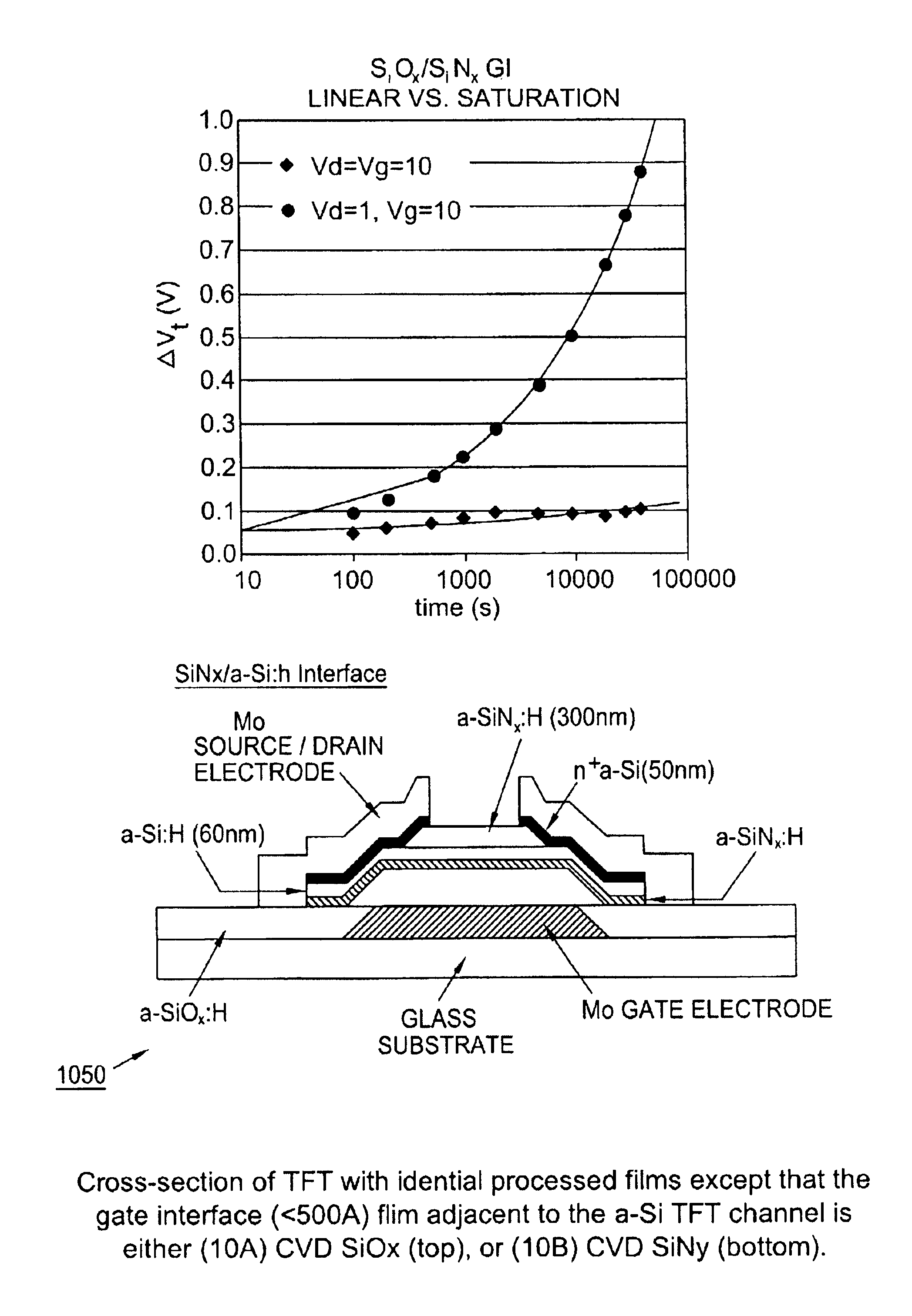
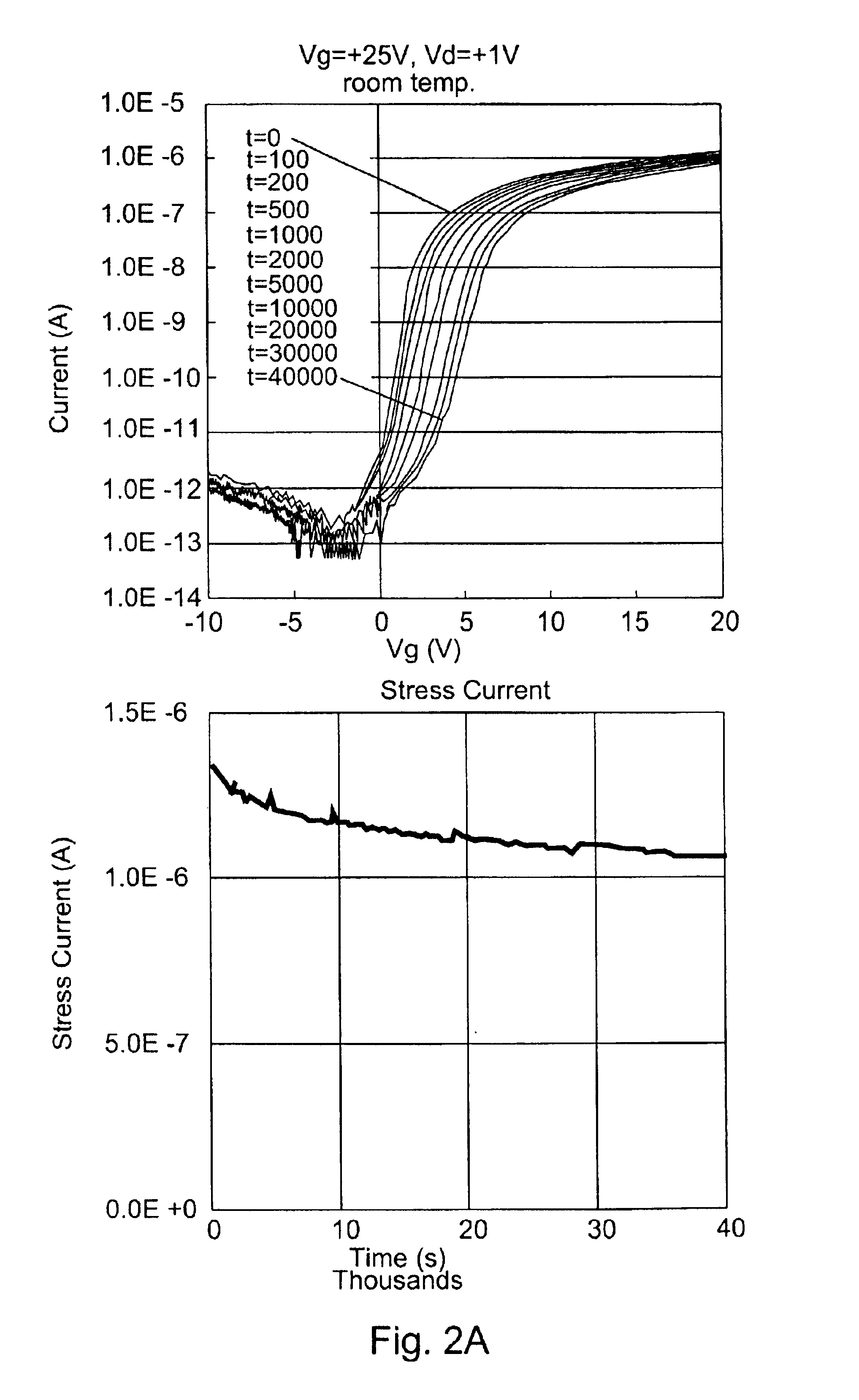
As a point of introduction, consider FIGS. 2A and 2B below. Both show threshold shift and drive current results for geometrically identical, neighboring TFTs from the same substrate, but in two quite different modes of operation. FIG. 2A shows the first TFT in the linear regime of operation with Vg=+25 V, and Vd=+1V (the source is grounded). FIG. 2B shows the neighboring TFT in the saturation regime with Vg=Vd=+10 V. Note that these voltages yield fairly similar drive currents, starting at approximately 1.40 μA for the TFT of FIG. 2a, and approximately 1.55 μA for the TFT in FIG. 2b. It is readily apparent that these conditions lead to dramatically different threshold stability in the nominally identical devices, namely, after 40,000 seconds of continuous (DC) stress at room temperature, the threshold shift (ΔVT) of the first TFT is approximately 4.0 V, while that of the second TFT is only approximately 0.25 V. It is clear that there are ranges of voltage which are clearly more suit...


PUM


Abstract

A circuit for providing a current to an organic light emitting diode comprising: (a) an amorphous silicon field effect transistor having a gate electrode and a drain electrode through which the current is provided to the organic light emitting diode; and (b) a controller for controlling a bias between the gate electrode and the drain electrode to maintain a threshold voltage shift of less than about 1V. The organic light emitting diode is preferably a component in an active matrix.

Description

The present invention is generally related to bias conditions and geometrical structures for amorphous silicon field effect transistors (FETs). More particularly, the present invention is directed to an amorphous silicon FET structure within a pixel that is directly supplying the current to the organic light emitting diode (OLED) and bias condition of that FET which reduces the threshold voltage instability with time and which does not degrade the performance of the device to deliver the needed current and gray scale. The resulting FET device and bias conditions are particularly useful in matrix addressed organic light emitting diodes (OLEDs).BACKGROUND OF THE INVENTIONDespite abundant conjecture to the contrary, it has been established for the first time that amorphous silicon (a-Si) technology is more than adequate to meet the pixel current drive requirements of an active matrix organic light-emitting diode (AMOLED) display. Prevailing wisdom, based almost exclusively on the indus...

Claims


Application Information

Patent Timeline
Patent Type & Authority Patents(United States)
IPC IPC(8): H01L29/66H01L29/786H01L29/40H01L29/49H01L27/32H01L27/28H05B44/00G09F9/30G09G3/20G09G3/30H01L51/50
CPCH01L29/78669H01L29/4908H01L27/3244G09G2310/0254H10K59/12H05B33/10H10K99/00
Inventor ANDRY, PAUL SLIBSCH, FRANK RTAKATOSHI, TSUJIMURA
Owner INNOLUX CORP
Why Eureka
Try Eureka