Method of sealing a hermetic lid to a semiconductor die at an angle

a technology of encapsulation and lid, applied in the field of encapsulation, can solve the problems of multiple reflections of light, lid to tilt, interference or diminishing the output signal of the mem device,

Inactive Publication Date: 2005-03-29
SILICON LIGHT MACHINES CORP
View PDF881 Cites 62 Cited by
  • Summary
  • Abstract
  • Description
  • Claims
  • Application Information

AI Technical Summary

Benefits of technology

In another embodiment of the invention, a portion of the first sealing ring is formed with channels and an overlapping portion of the second complimentary sealing ring is also formed with channels. A suitable solder material is placed between the first and second sealing ring and caused to flow, as described above. The additional surface tension created by the channels causes the solder layer to be thinner in the channel regions forming an asymmetric seal causing the lid to tilt.

Problems solved by technology

The hermetic and transparent lids have at least two interfaces which can result in several and multiple reflections of light and interfere or diminish the output signal of the MEM device.
Regions where the sealing rings have edge or side wetting surface(s), thereby producing an asymmetric surface tension and causing the lid to tilt.

Method used


Image

  • Method of sealing a hermetic lid to a semiconductor die at an angle
  • Method of sealing a hermetic lid to a semiconductor die at an angle
  • Method of sealing a hermetic lid to a semiconductor die at an angle

Examples


Embodiment Construction

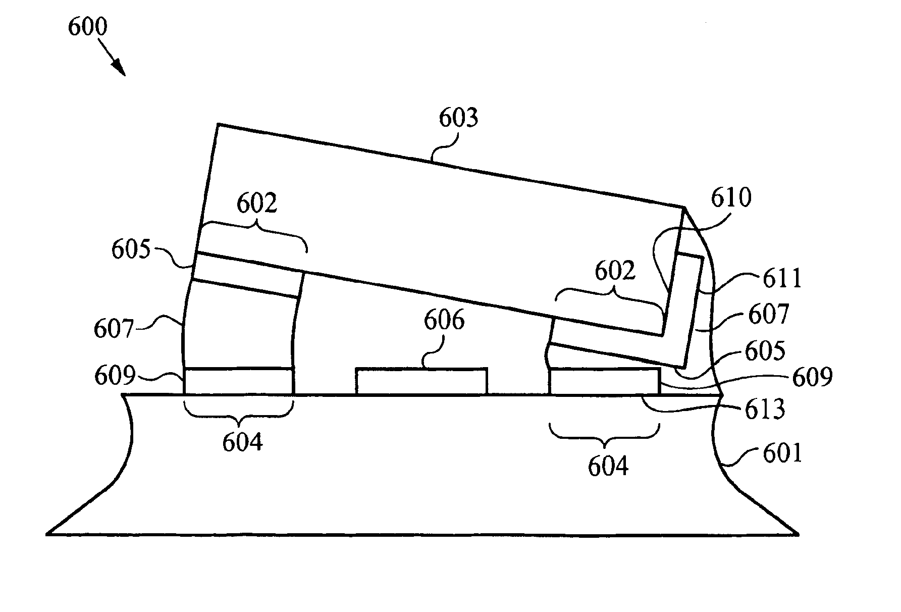
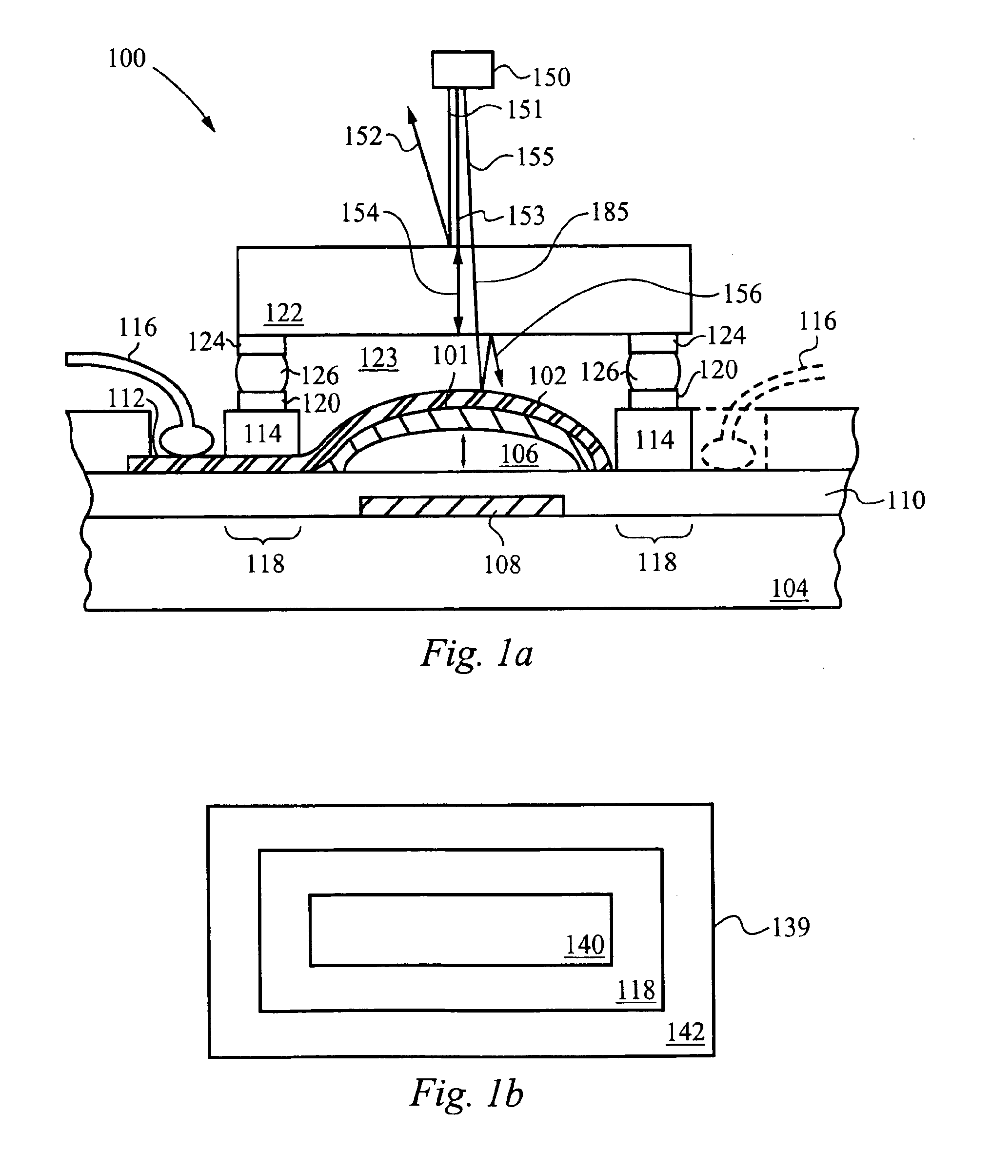
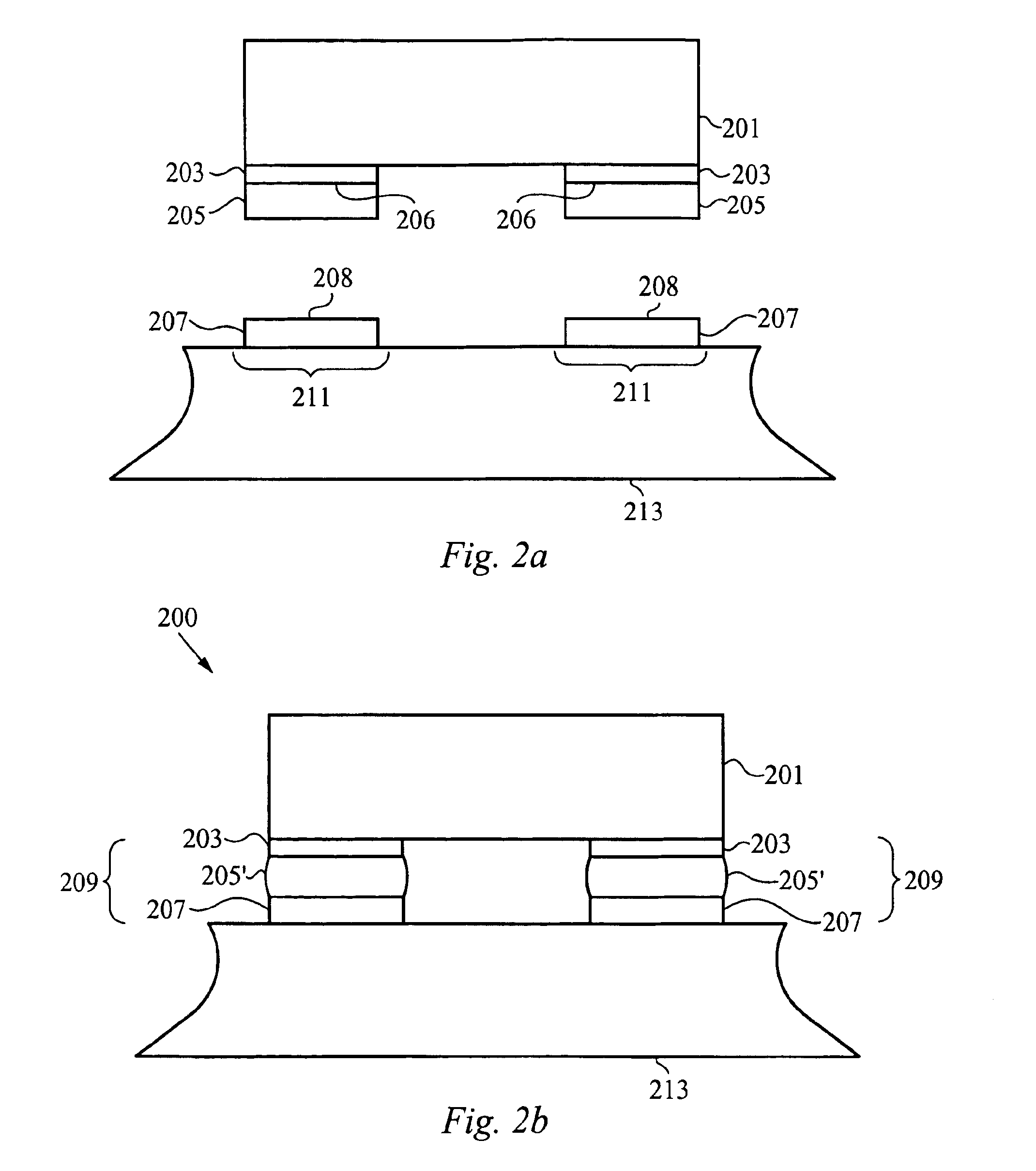
The present invention is directed to providing a hermetical seal between an optical window or lid, that is preferably formed from glass or other transparent material, and a substrate or die structure, that is preferably formed from a silicon-based material. The lid and the substrate preferably encapsulate a mechanically active portion of an optical MEM device. In accordance with the invention, the lid is positioned at an angle relative to the mechanically active portion, substrate, or both through an asymmetric seal in order to reduce reflections, which can interfere the MEM device signal and / or image. While the present invention is preferably directed to providing an asymmetric seal in optical MEM devices, the present invention can also be used to control the orientation and / or position of any number of micro-structures relative to each other by forming an asymmetric solder seal or joint.

An optical MEM device of the present invention can be a diffraction grating light valve compris...


PUM


Abstract

The current invention provides a optical MEM device and system with an angled lid for hermetically sealing an active MEMS structure. The lid is sealed through an asymmetric seal formed with sealing rings having an asymmetric distribution of solder wetting surfaces which tilts the lid, when the lid and a substrate are soldered together. The asymmetric distribution wetting surfaces can be provided by forming one or more edge features, by patterning portions of the sealing rings or both. Preferably, the lid is transparent to one or more wavelengths of light in a range of 300 to 3000 Angstroms and hermetically seals a grating light valve structure having a plurality of movable ribbon for modulating light through the lid.

Description

FIELD OF THE INVENTIONThis invention relates to the field of encapsulation, especially hermetically. More particularly, this invention relates to the encapsulation of MEM devices with a lid structure.BACKGROUND OF THE INVENTIONIn the manufacture of integrated circuits (chips) it is well known that it is desirable to encapsulate the chip in order to protected the chip from mechanical damage and contamination. Encapsulation techniques are also known to passivate the chips an enhance their long term performance. There are a variety of well known techniques available for encapsulating chips. These techniques include mounting chips within a cavity of a substrate or a die structure, wire bonding chips to a lead frame and then enclosing the package with a lid. Another technique includes mounting chips to a lead frame, wire bonding the chips to the lead frame and then passivating the chips and a portion of the lead frame in a molded plastic or plastic epoxy body. Yet another technique for p...

Claims


Application Information

Patent Timeline
Patent Type & Authority Patents(United States)
IPC IPC(8): B81B7/00H01L21/00H01L21/50H01L21/02
CPCB81B7/0067H01L21/50H01L21/67126H01L2224/1403H01L2224/0401H01L2224/0603
Inventor LEUNG, OMAR S.
Owner SILICON LIGHT MACHINES CORP
Why Eureka
Try Eureka