Method and apparatus for predicting semiconductor device lifetime

Inactive Publication Date: 2005-03-29
ADVANCED MICRO DEVICES INC
View PDF14 Cites 27 Cited by
  • Summary
  • Abstract
  • Description
  • Claims
  • Application Information

AI Technical Summary

Problems solved by technology

As electrons flow in the channel, some scattering of the electrons in the lattice of the silicon substrate occurs due to interface states and fixed charges (interface defects).
Over a period of time, hot carriers degrade the silicon bonds with an attendant increase in electron scattering due to an increase in interface and bulk defects.
As a res

Method used


Image

  • Method and apparatus for predicting semiconductor device lifetime
  • Method and apparatus for predicting semiconductor device lifetime
  • Method and apparatus for predicting semiconductor device lifetime

Examples


Embodiment Construction

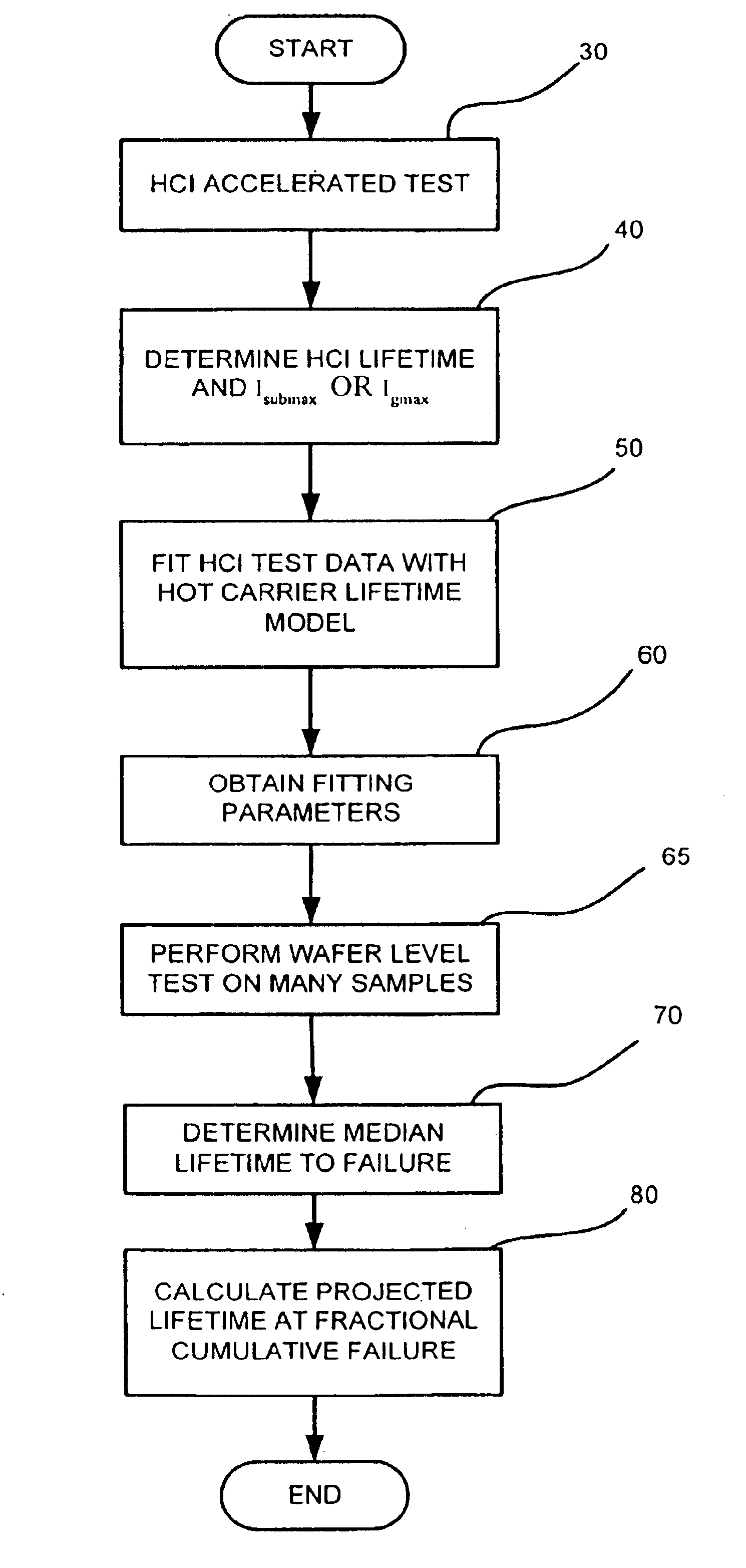
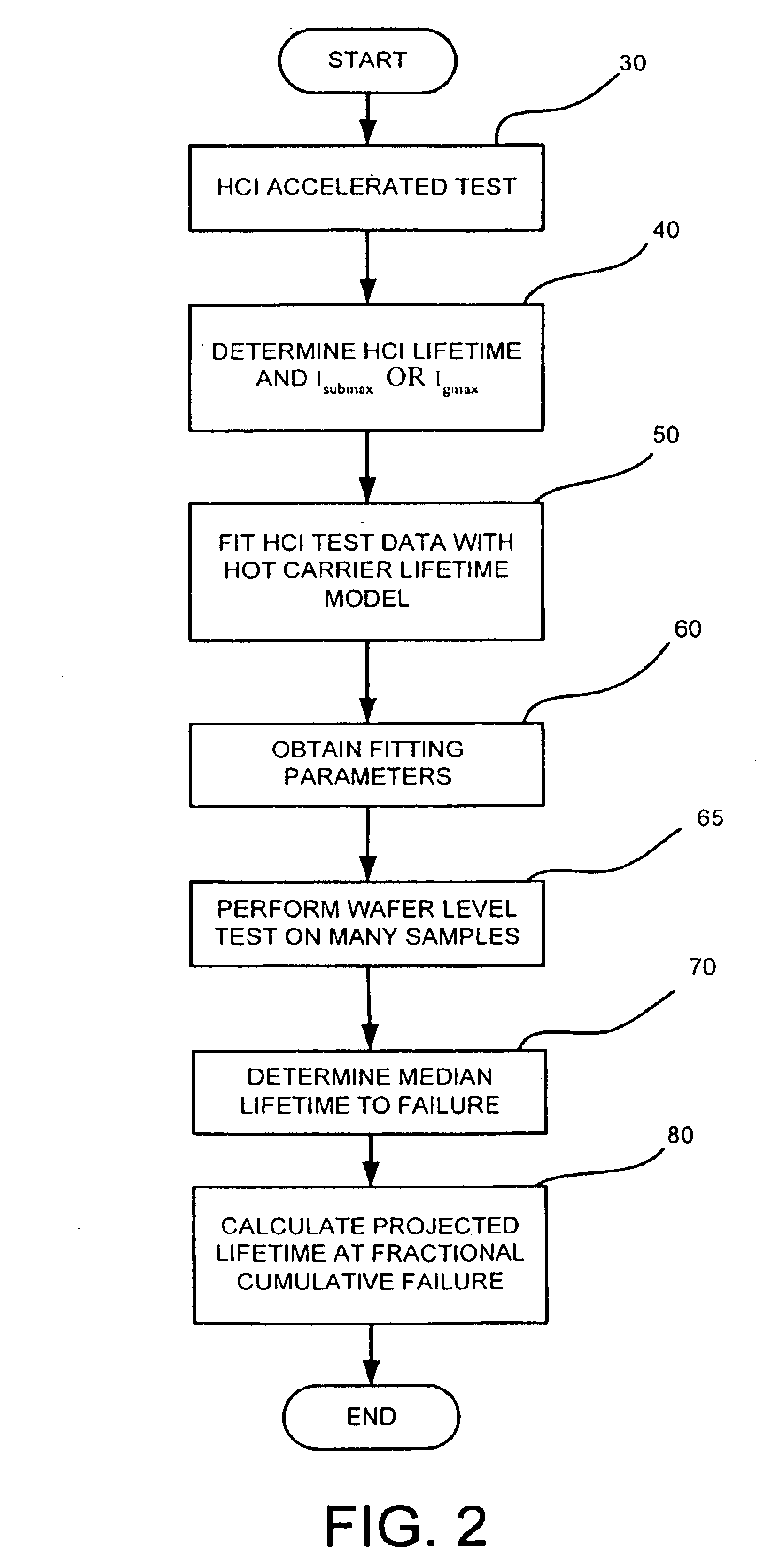
In accordance with the present invention, a method and apparatus for predicting a semiconductor device lifetime is provided. More specifically, the present invention relates to a comprehensive DC HCI lifetime projection model. The present invention provides a more precise lifetime prediction with improvement in lot to lot, wafer to wafer distribution.

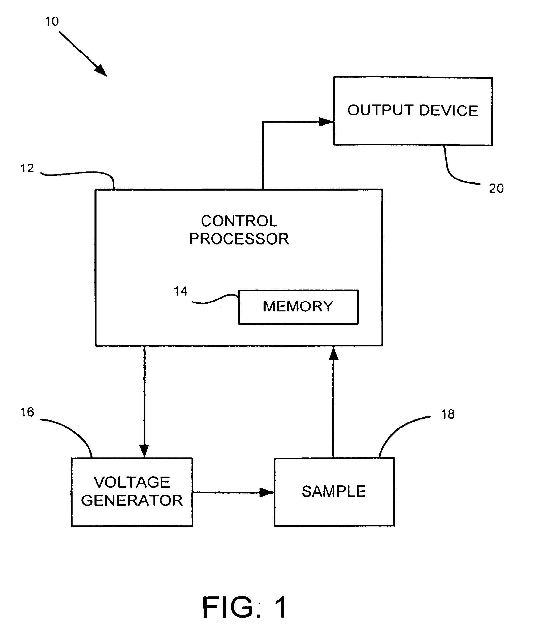
Referring now to FIG. 1, a system 10 that is suitable for carrying out a method of predicting a lifetime of a semiconductor device is illustrated. The system 10 can include a control processor 12, such as a computing device, containing a memory 14. The control processor 12 is operative to provide control signals to a voltage generator 16 for performing testing operations on a sample 18 in a manner described more fully below. Data can be collected from the sample 18 and processed appropriately by the control processor 12. Suitable output can be provided to an output device 20, such as, for example, a computer monitor, printer, and the li...


PUM


Abstract

A method of predicting a lifetime of a semiconductor device at a predetermined operating condition includes performing a hot carrier injection (HCI) accelerated stress test on a plurality of MOS transistors. For each HCI test, a HCI lifetime and a maximum substrate or gate current are determined. The HCI test data is fit with a hot carrier lifetime model and fitting parameters are obtained. A wafer level test is performed on at least 10N transistors in which a maximum substrate or gate current is determined for each transistor. A median lifetime to failure is determined for the statistical distribution of maximum substrate or gate current values at the predetermined operating condition. From the determined median lifetime to failure, a projected lifetime at a fractional cumulative failure is calculated.

Description

TECHNICAL FIELDThe present invention relates to a method of estimating HCI lifetime in a MOS transistor, and to a comprehensive DC HCI lifetime projection model. More specifically, it relates to an improved method and apparatus for predicting semiconductor device lifetimes.BACKGROUND ARTAs devices have been scaled, the channel length in the semiconductor devices has become smaller and smaller. When the semiconductor devices have a gate size of 0.13 micron, for example, the extremely short channel length generates a hot carrier effect. For example, as the channel length is made smaller, it's associated electric field increases. As the electric field increases, the force on the electrons increases causing them to move faster and faster in the channel. Such energetic electrons are referred to as “hot carriers”.There is a potential barrier between the silicon substrate and the silicon dioxide (SiO2) gate oxide of a metal oxide semiconductor (MOS) transistor. As electrons flow in the cha...

Claims


Application Information

Patent Timeline
IPC IPC(8): G06F11/30G21C17/00G01R31/28
CPCG01R31/287G01R31/2858
Inventor KIM, HYEON-SEAG
Owner ADVANCED MICRO DEVICES INC
Why Eureka
Try Eureka