Integration scheme using self-planarized dielectric layer for shallow trench isolation (STI)

a dielectric layer and self-planarized technology, applied in the field of integrated circuit fabrication, can solve the problems of increasing the thickness of the trench, increasing the cost and complexity of the installation, and requiring expensive equipment, so as to the electrical characteristics of the device, and improve the quality of the trench fill layer

Inactive Publication Date: 2005-04-05
APPLIED MATERIALS INC
View PDF7 Cites 27 Cited by
  • Summary
  • Abstract
  • Description
  • Claims
  • Application Information

AI Technical Summary

Benefits of technology

Specific embodiments of the present invention provide more efficient methods for providing shallow trench isolation integration by forming self-planarized, high quality trench fill layers using surface sensitive dielectric materials. The invention does so by depositing a polysilicon layer prior to etching the isolation trenches

Problems solved by technology

The reverse mask and etch procedure necessitated by the step height effect adds significant cost and complexity (for example, due to the added lithography steps involved) to the planarization procedure.
From the discussion above, it is seen that multiple steps, including additional photolithography steps (which require expensive equipment), are needed to provide STI.
However, lowering the O3/TEOS ratio tends to undesirably result in a more porous dielectric film.
This is particularly problematic when the dielectric film is used for isolation purposes

Method used


Image

  • Integration scheme using self-planarized dielectric layer for shallow trench isolation (STI)
  • Integration scheme using self-planarized dielectric layer for shallow trench isolation (STI)
  • Integration scheme using self-planarized dielectric layer for shallow trench isolation (STI)

Examples


Embodiment Construction

I. Self-Planarized Deposition of a Dielectric Layer in Shallow Trench Integration

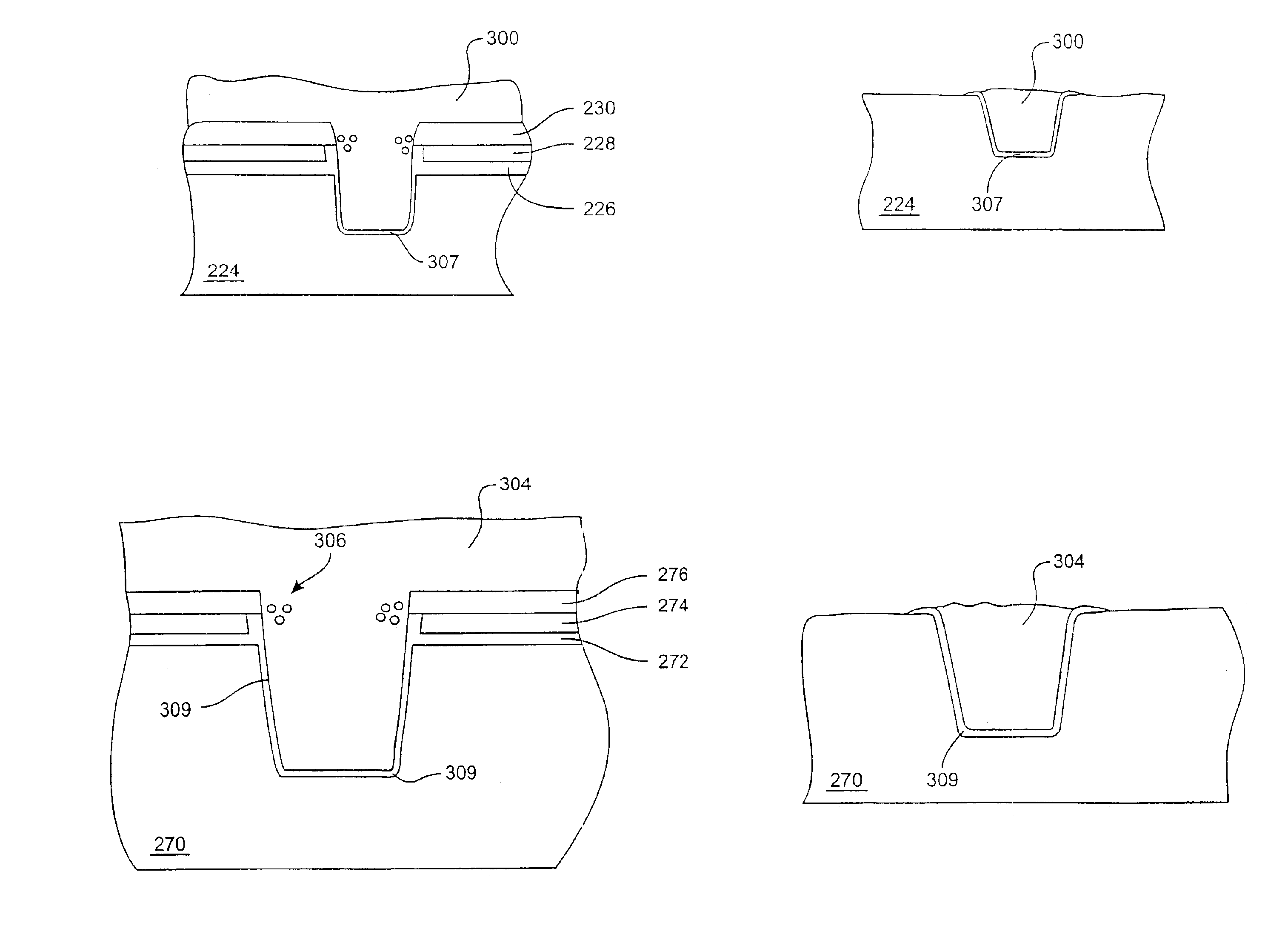
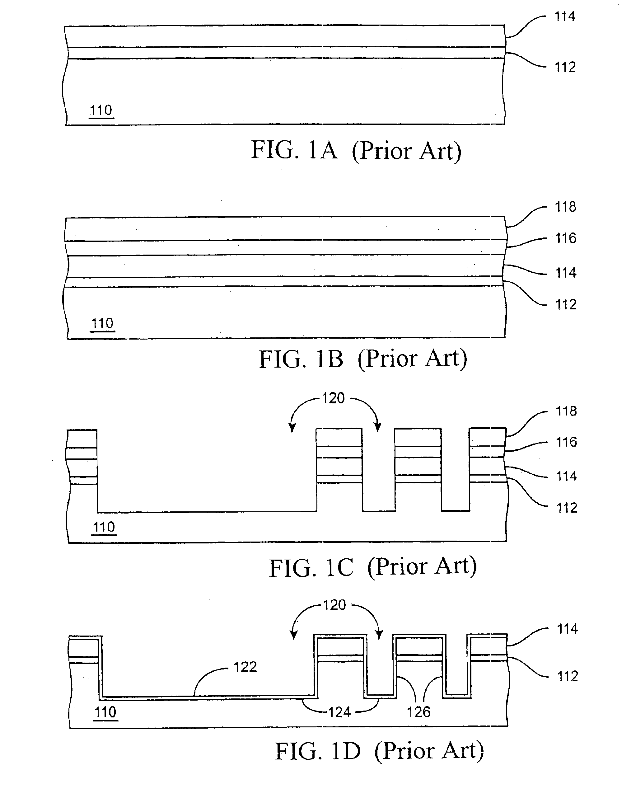
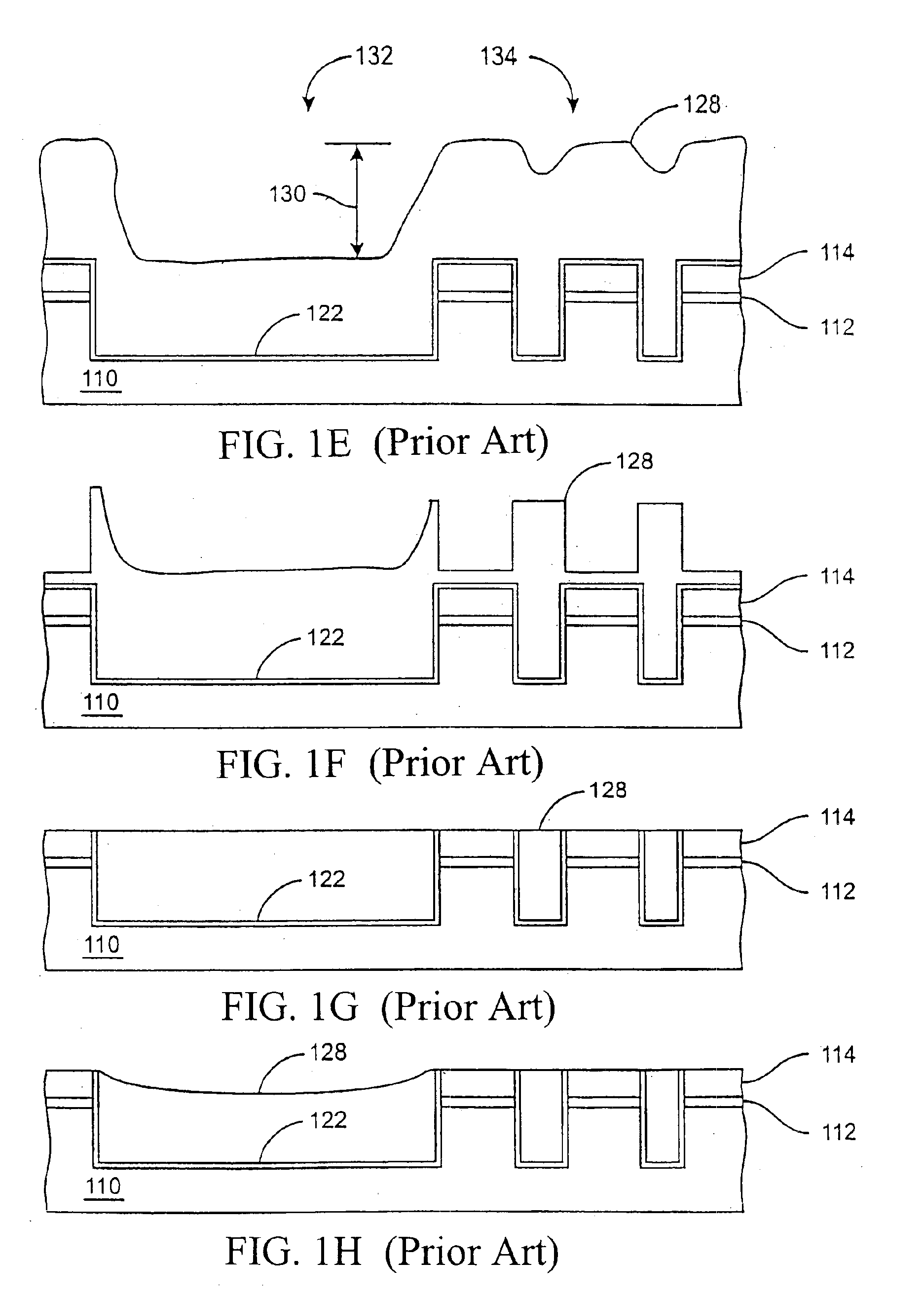
Specific embodiments of the present invention are illustrated using an STI integration as an example. The benefits of the various embodiments of the invention can be readily seen by comparison with the prior art methods, such as illustrated in FIGS. 1A-1H. Specifically, the present invention provides more efficient shallow trench isolation integration by providing self-planarized deposition of a dielectric trench fill layer without sacrificing the quality of the dielectric layer. The present invention further provides dielectric trench fill layers which have undesirable porous regions removed by CMP. It is understood that the scope of the invention is not necessarily limited to STI integration.

A. Forming a Trench

FIGS. 3A and 3B illustrate alternate methods of forming a trench on a substrate, typically a silicon substrate. Referring to FIG. 3A, the first step 202 is to apply a pad oxide directly on the s...


PUM

PropertyMeasurementUnit
Temperatureaaaaaaaaaa

Abstract

A method for forming a trench isolation structure on a substrate. The method includes applying a pad oxide layer (226) on the substrate (224), applying a polysilicon layer (228) over the pad oxide layer, and applying a CVD anti-reflective coating (ARC) (230) over the polysilicon layer. A photoresist is formed on the CVD ARC and a trenched is etched at a desired location. One embodiment provides a method for depositing a trench oxide filling layer (300) on the trenched substrate utilizing the surface sensitivity of dielectric materials such as O3/TEOS to achieve a substantially self-planarized dielectric layer. Prior problems with porous trench fill, particular near trench corners, are obviated by use of the polysilicon layer. After deposition, an oxidizing anneal can be performed to grow a thermal oxide (307) at the trench surfaces and densify the dielectric material. A chemical mechanical polish can be used to remove the excess oxide material, including the porous regions.

Description

BACKGROUND OF THE INVENTIONThe present invention relates to the fabrication of integrated circuits. More particularly, the present invention is directed toward methods for providing self-planarized deposition of high quality dielectric layers for shallow trench isolation.Semiconductor device geometries continue to decrease in size, providing more devices per unit area on a fabricated wafer. These devices are typically initially isolated from each other as they are built into the wafer, and they are subsequently interconnected to create the specific circuit configurations desired. Currently, some devices are fabricated with feature dimensions as small as, or smaller than, 0.18 μm. For example, spacing between devices such as conductive lines or traces on a patterned wafer may be separated by 0.18 μm leaving recesses or gaps of a comparable size. A nonconductive layer of dielectric material, such as silicon dioxide (SiO2), is typically deposited over the features to fill the aforement...

Claims


Application Information

Patent Timeline
IPC IPC(8): H01L21/70H01L21/762H01L21/285H01L21/027H01L21/02H01L21/3105H01L21/316C23C16/04C23C16/40
CPCC23C16/045C23C16/402H01L21/76229H01L21/0276H01L21/31053H01L21/31612H01L21/31662H01L21/28525H01L21/02164H01L21/02238
Inventor GAILLARD, FREDERICGEIGER, FABRICEYIEH, ELLIE Y.
Owner APPLIED MATERIALS INC
Why Eureka
Try Eureka