Method of manufacturing high coupling ratio flash memory having sidewall spacer floating gate electrode

a floating gate electrode and high coupling ratio technology, applied in the direction of semiconductor devices, basic electric elements, electrical appliances, etc., can solve the problems of non-symmetrical memory cell programming, data read-out errors, net positive charge, etc., and achieve the effect of slowing down the operating speed and improving the overall performance of memory cells

Inactive Publication Date: 2005-04-05
POWERCHIP SEMICON MFG CORP
View PDF8 Cites 31 Cited by
  • Summary
  • Abstract
  • Description
  • Claims
  • Application Information

AI Technical Summary

Benefits of technology

Accordingly, one object of the present invention is to provide a method of manufacturing a flash memory. A self-aligned process is utilized to fabricate a floating gate so that a slow down of the operating speed resulting from a non-symmetrical programming of memory cell in the presence of channels with unequal lengths are prevented. Hence, overall performance of the memory cells is improved.

Problems solved by technology

Since the quantity of electrons bled out from the floating gate when erasing data from the flash memory is difficult to control, an excessive amount of electrons may flow out from the floating gate resulting in a net positive charge.
When over-erase is excessive, the channel underneath the floating gate may conduct before the application of an operating voltage to the control gate and hence ultimately lead to a data read-out error.
Because channel length of two neighboring memory cells using the same common source region are non-identical, memory cell programming will be non-symmetrical.

Method used


Image

  • Method of manufacturing high coupling ratio flash memory having sidewall spacer floating gate electrode
  • Method of manufacturing high coupling ratio flash memory having sidewall spacer floating gate electrode
  • Method of manufacturing high coupling ratio flash memory having sidewall spacer floating gate electrode

Examples


first embodiment

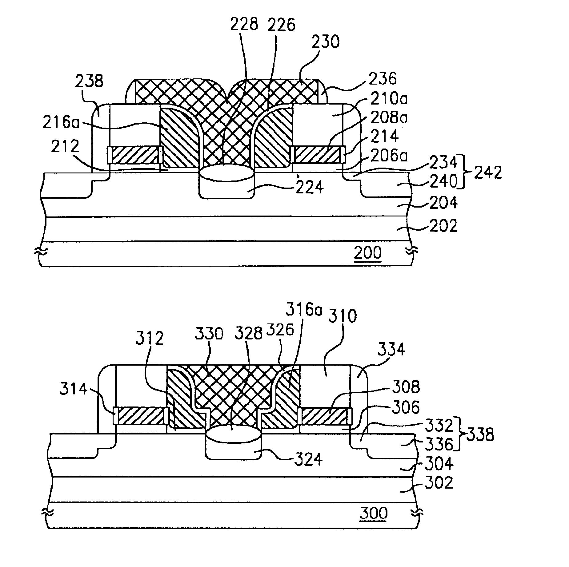
In this invention, the floating gate (the conductive layer 216a) is formed in a self-aligned process and hence the channel of two neighboring memory cell has equal length. Since channel length of two neighboring memory cells using the same source region is identical, non-symmetrical memory cell programming is prevented and reliability of the memory is improved.

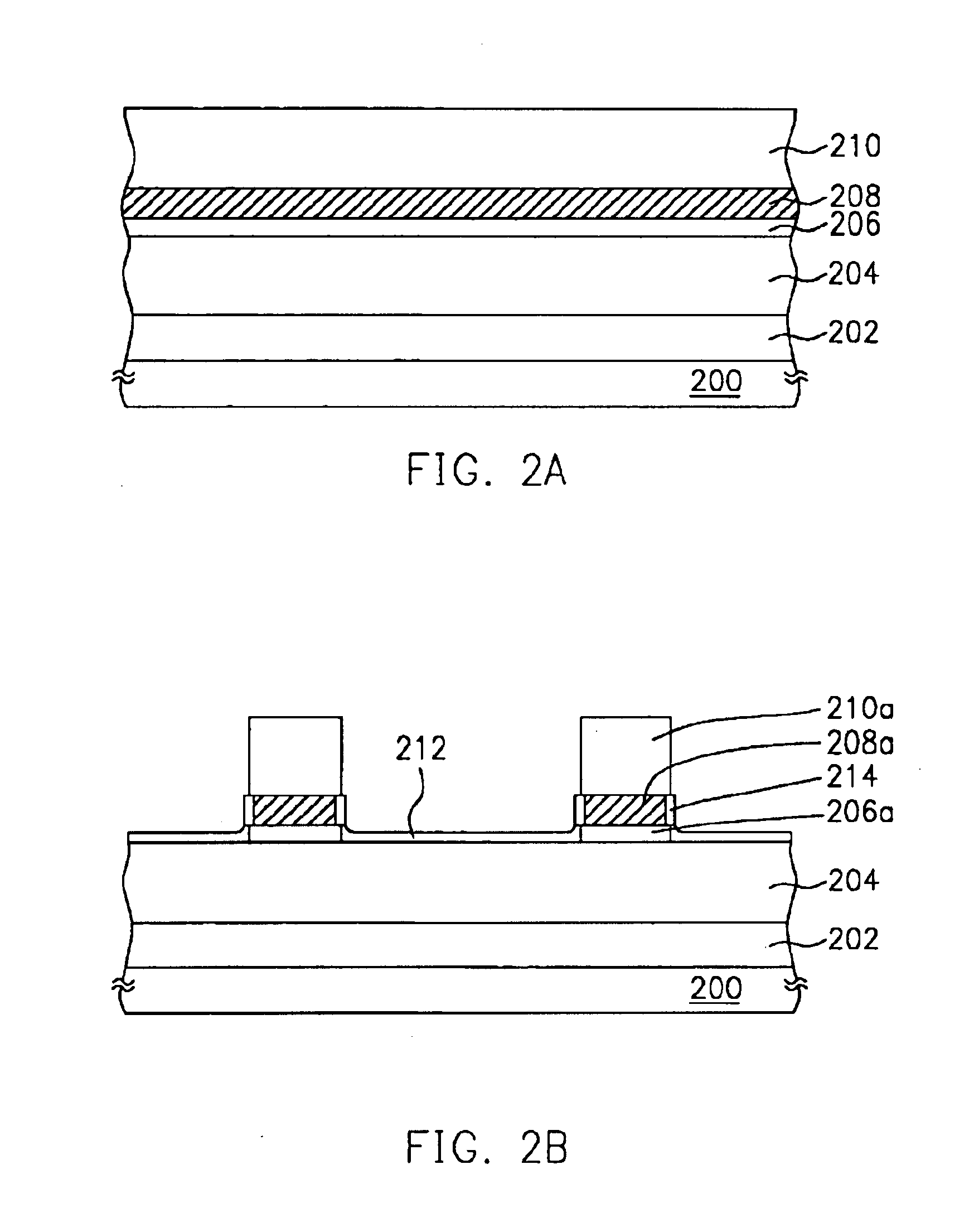
FIGS. 3A to 3D are schematic cross-sectional views showing the steps for producing a flash memory according to a second preferred embodiment of this invention. As shown in FIG. 3A, a substrate 300 such as a P-type silicon substrate is provided. The substrate 300 has a deep N-well region 302 and a P-well region 304 above the deep N-well region 302. Thereafter, according to FIGS. 2A and 2B, a dielectric layer 306, a conductive layer 308 and a cap layer 310, a tunneling oxide layer 312 and spacers 314 are sequentially formed over the substrate 300. The cap layer 310, the conductive layer 308 and the dielectric layer 306 together ...

second embodiment

In this invention, the floating gate (the conductive layer 316a) is formed in a self-aligned process and hence the channel of two neighboring memory cell has equal length. Since channel length of two neighboring memory cells using the same source region is identical, non-symmetrical memory cell programming is prevented and reliability of the memory is improved.

Furthermore, because the floating gate (the conductive layer 316a) has an L-shaped profile, overlapping area between the floating gate (the conductive layer 316a) and the control gate (the conductive layer 330) is increased. Since gate coupling ratio of the device increases with overlapping area, overall performance of the device will improve.


PUM


Abstract

A method of manufacturing a flash memory is provided. First, a substrate with a first gate structure and a second gate structure thereon is provided. The first gate structure and the second gate structure each comprises of a dielectric layer, a first conductive layer and a cap layer. A tunneling oxide layer is formed over the substrate and then a first spacer is formed on the sidewall of the first conductive layer. Thereafter, a second conductive layer is formed on one side designated for forming a source region of the sidewalls of the first gate structure and the second gate structure. Then, the source region is formed in the substrate in the designated area. Next, an inter-gate dielectric layer is formed over the second conductive layer and then an insulating layer is formed over the source region. After forming a third conductive layer over the area between the first gate structure and the second gate structure, a drain region is formed in the substrate.

Description

BACKGROUND OF THE INVENTION1. Field of InventionThe present invention relates to a semiconductor manufacturing method. More particularly, the present invention relates to a method of manufacturing a flash memory.2. Description of Related ArtFlash memory is a type of device that permits multiple accesses, read-outs and erases. Furthermore, data stored within the device is retained even after power to the device is cut off. With such big advantages, flash memory is one of the most useful non-volatile memories in personal computers and electronic equipment.A typical flash memory device has doped polysilicon floating gate and control gate. The floating gate and the control gate inside the device are isolated from each other by a dielectric layer. To write / erase data into a flash memory, a bias voltage is applied to the control gate and the source / drain region and hence electrons are injected into the floating gate or pulled out of the floating gate. To read data from the flash memory, a...

Claims


Application Information

Patent Timeline
Patent Type & Authority Patents(United States)
IPC IPC(8): H01L21/70H01L27/115H01L21/8247
CPCH01L27/11521H01L27/115H10B69/00H10B41/30
Inventor HUNG, CHIH-WEIHSU, CHENG-YUANSUNG, DA
Owner POWERCHIP SEMICON MFG CORP
Why Eureka
Try Eureka