

Masking layer in substrate cavity
a masking layer and substrate technology, applied in the field of microelectrooptical system packaging, can solve the problems of destroying the packaging device, the packaging cavity cannot be filled with potting compound, and other types of packaging have not yet been commercially viable, so as to prevent particle generation
- Summary
- Abstract
- Description
- Claims
- Application Information
AI Technical Summary
Benefits of technology
Problems solved by technology
Method used
Image

Examples
Embodiment Construction
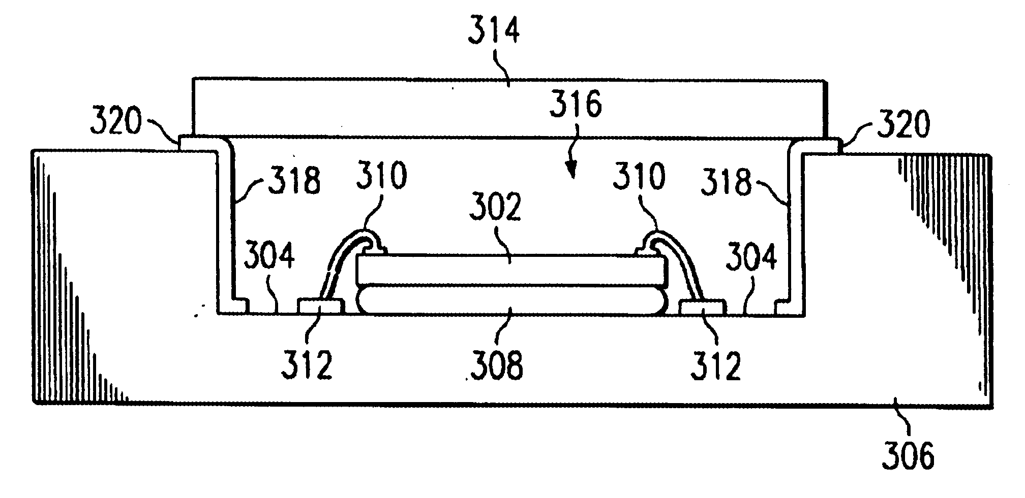
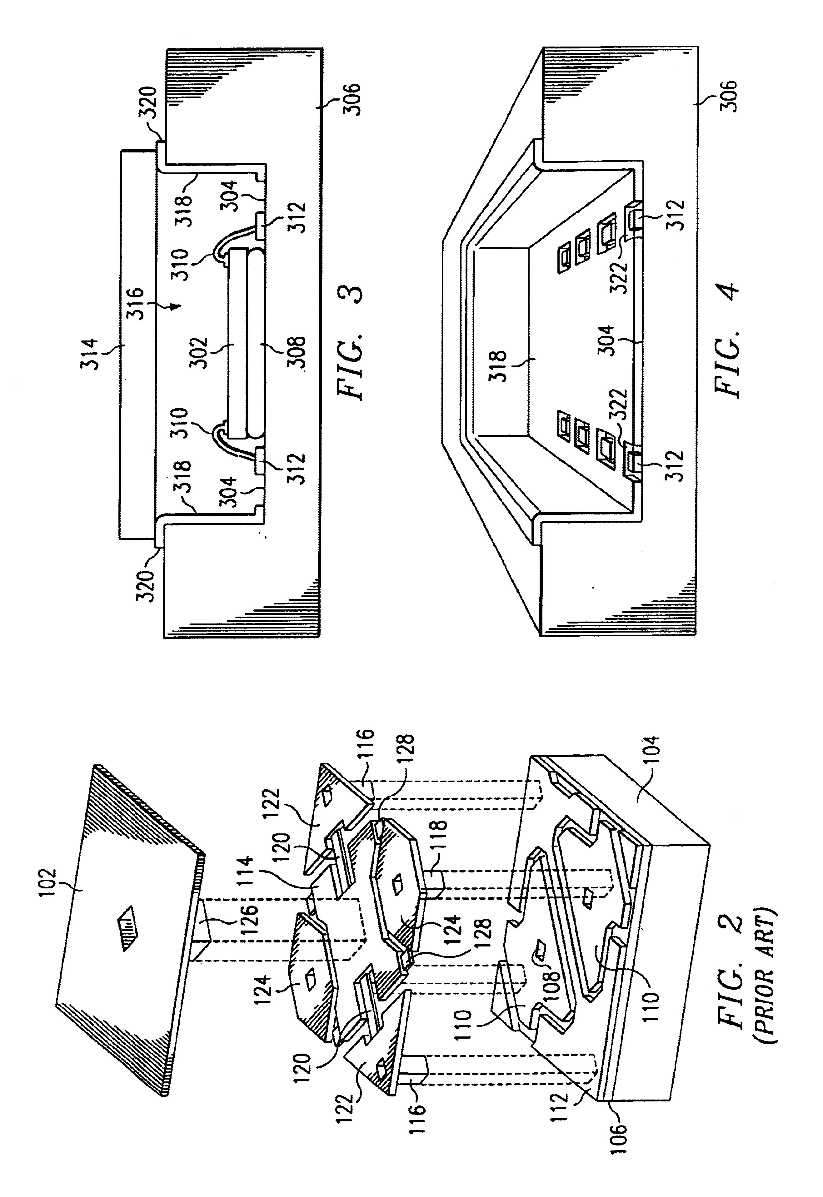
The present invention provides an improved package and package substrate that is useful for packaging of MEMS devices. Particle generation by the substrate is reduced by the application of a liner over the inner ceramic surfaces. The liner is particularly useful when applied over the rough edges of the substrate cavity wall and over the sharp edges of the substrate.
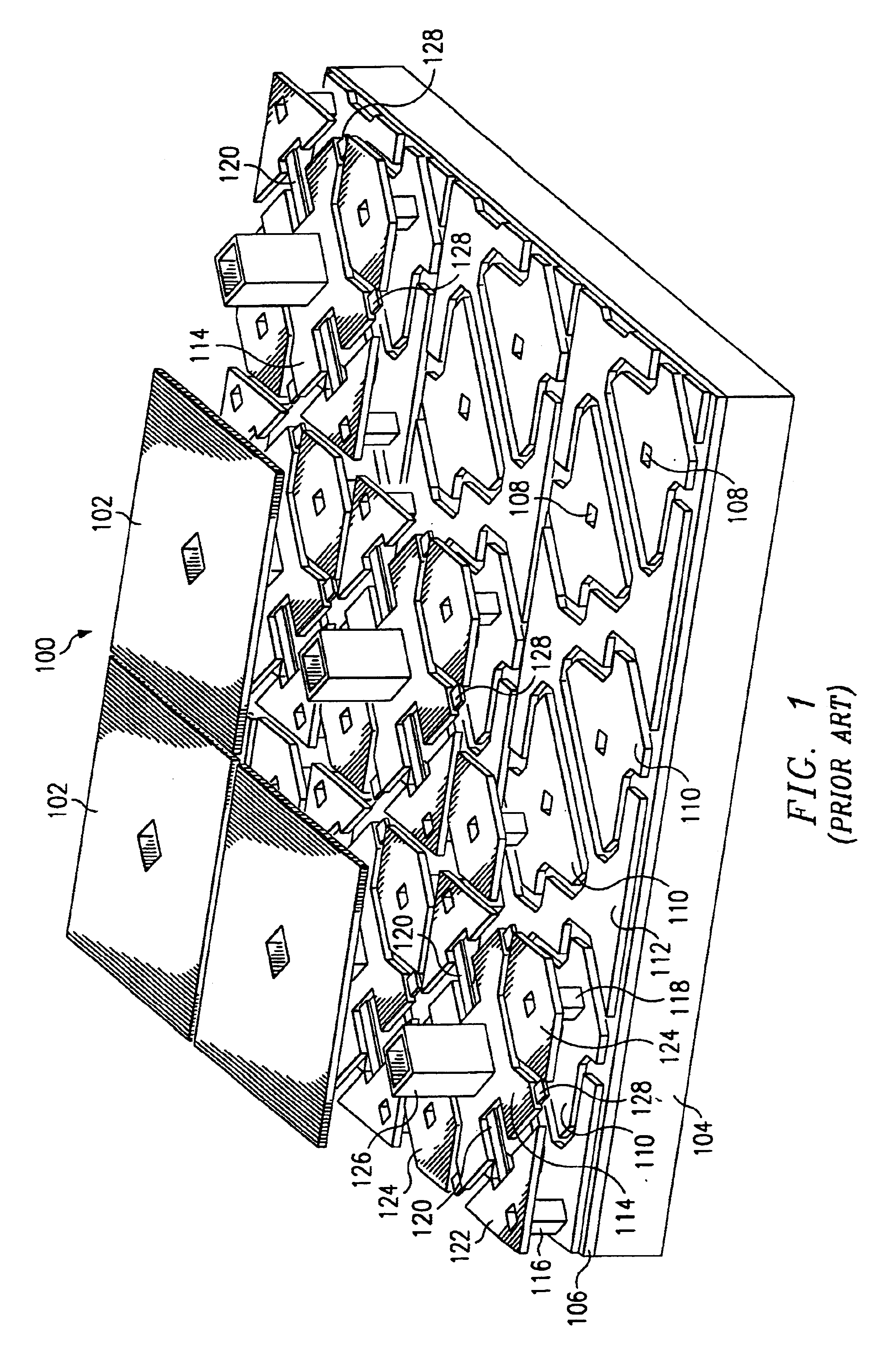
The improved package substrate of the present invention is particularly useful when used to package micromirror devices such as the one shown in FIGS. 1 and 2. As shown in FIG. 1, a typical hidden-hinge micromirror 100 is actually an orthogonal array of micromirror cells, or elements. This array often includes more than a thousand rows and columns of micromirrors. FIG. 1 shows a small portion of a micromirror array of the prior art with several mirrors 102 removed to show the underlying mechanical structure of the micromirror array. FIG. 2 is an exploded view of a single micromirror element of the prior art further detail...
PUM
 Abstract
Description
Claims
Application Information