Organic electroluminescent device

an electroluminescent device and organic technology, applied in the direction of vacuum evaporation coating, chemical vapor deposition coating, coating, etc., can solve the problems of affecting the performance of the organic electroluminescent element is remarkably degraded, and the materials used are limited, so as to achieve high precision and fine patterning, and simple process without restricting the structure of the electroluminescent devi

Inactive Publication Date: 2005-04-12
TORAY IND INC
View PDF12 Cites 68 Cited by
  • Summary
  • Abstract
  • Description
  • Claims
  • Application Information

AI Technical Summary

Benefits of technology

The object of the present invention is to solve the above problems by providing a method for producing an organic electroluminescent device which allows highly precise fine patterning under various vapor deposition conditions without degrading the properties of the organic electroluminescent elements and can achieve high stability by a relatively simple process without limiting the structure of the electroluminescent device.

Problems solved by technology

However, the above mentioned conventional methods have the following problems.
According to said photolithographic method, since the organic thin film, layer used as a component of an organic electroluminescent element is generally poor in the durability against water, organic solvents and chemical solutions, the performance of the organic electroluminescent element is remarkably degraded.
Furthermore, to obtain an organic electroluminescent element allowing the application of a wet process, the materials used are limited.
According to the partition methods, since patterning is achieved by using the shadows of the deposit formed by partitions, highly precise patterning cannot be achieved when vapor deposition is effected at various angles or when vapor strays behind the partitions in a large quantity.
So, these methods are not suitable for larger substrate areas, higher vapor deposition rates or more highly precise patterning.
Furthermore, since regions free from the second electrodes called dead spaces corresponding to the shadows of the deposit exist on the organic thin film layer, the organic electroluminescent element tends to be deteriorated by the invasion of water, etc. from there.
Moreover, it is not easy to stably form partitions with a large sectional aspect ratio and specially formed partitions with overhangs on the entire surface of the substrate.
In the conventional masking methods, the vapor strays due to the poor contact between the substrate and the shadow mask.
Especially when a shadow mask extremely narrow in the mask portion compared to the apertures is used, for example, for patterning second electrodes formed in stripes, the apertures can be deformed due to insufficient strength of the shadow mask.
So, it is difficult to highly precisely achieve the fine patterning in sub-millimeter ranges required for displays, etc.

Method used


Image

  • Organic electroluminescent device
  • Organic electroluminescent device
  • Organic electroluminescent device

Examples


example 1

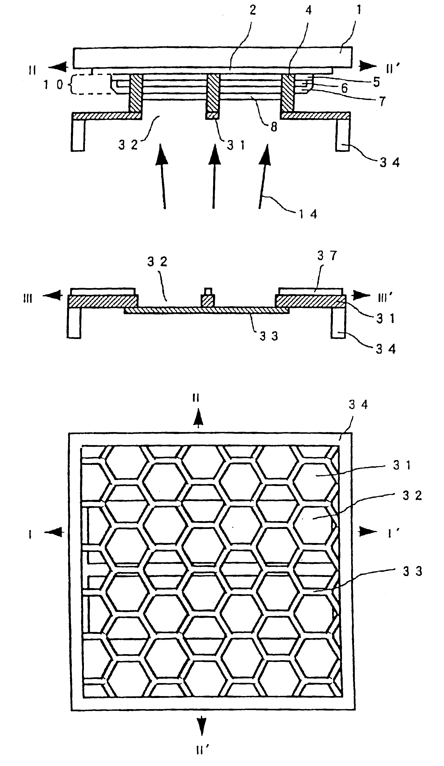
Shadow masks with a structure in which the mask portion and the reinforcing lines were formed on the same plane as shown in FIG. 17 were prepared for patterning the emitting layer. Each of the shadow masks was 120×84 mm in outside form and 25 μm in the thickness of the mask portion 31, and had ninety two 64 mm long 305 μm wide apertures 32 formed in stripes at a pitch of 900 μm in the crosswise direction. At the apertures formed in stripes, 20 μm wide and 25 μm thick reinforcing lines 33 across the apertures were formed at 1.8 mm intervals. Furthermore, the shadow mask was fixed on a 4 mm wide stainless steel frame 34 equal in outside form to the shadow mask.

A shadow mask with a structure in which a clearance 36 was formed between one face 35 of a mask portion 31 and reinforcing lines 33 as shown in FIGS. 30 and 31 was prepared for patterning the second electrodes. The shadow mask was 120×84 mm in outside form and 170 μm in the thickness of the mask portion, and had sixty six 100 mm...

example 2

The process till the formation of the hole transport layer was the same as described for Example 1.

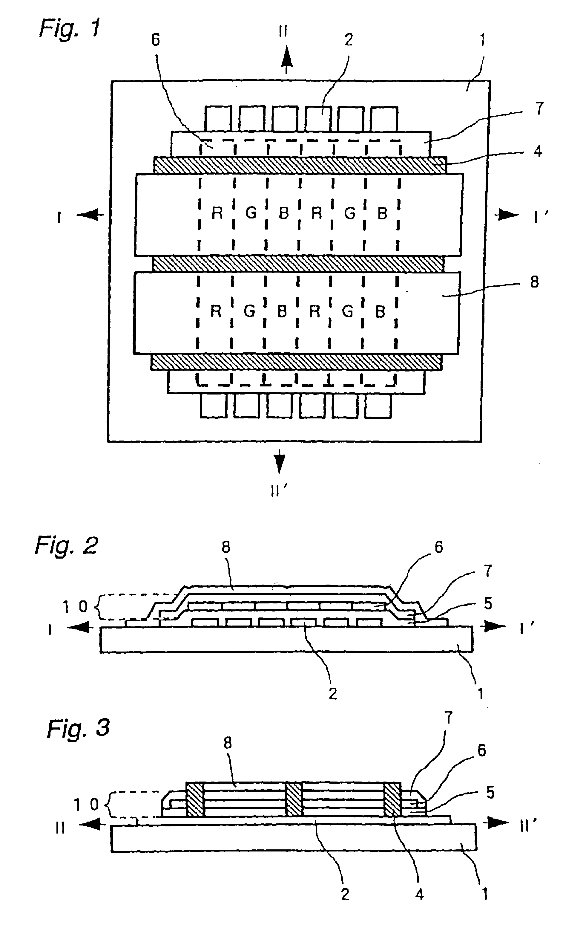
Then, a first shadow mask for the emitting layer was arranged before the substrate, and they were kept in contact with each other. Behind the substrate, a ferrite magnetic shell (YMB-1B produced by Hitachi Metals, Ltd.) was arranged. In this case, as shown in FIGS. 18 and 19, the shadow mask and the substrate were positioned to ensure that the first electrodes 2 formed in stripes were located at the centers of the apertures 32 formed in stripes in the shadow mask, and that the reinforcing lines 33 agreed with the spacers 4 in position and were kept in contact with the spacers. In this state, Alq3 was vapor-deposited by 30 nm, to pattern the G regions of the emitting layer. Then, as described for patterning the G regions of the emitting layer, a second shadow mask for the emitting layer was used to deposit Alq3 with 1 wt % of DCM doped by 40 nm, for patterning the R regions of the emitt...

example 3

As described for Example 1, the ITO was patterned as first electrodes in 90 mm long and 280 μm wide stripes, and the photoresist was removed. As described for Example 1, 272 first electrodes were formed in strips on a glass substrate at a pitch of 300 μm in the crosswise direction.

The spacers were formed as described below. Glycidyl methacrylate was added to a copolymer consisting of 40% of methacrylic acid, 30% of methyl methacrylate and 30% of styrene by 0.4 equivalent for each equivalent of the carboxyl groups of the copolymer for reaction, to obtain an acrylic copolymer with carboxyl groups and ethylene unsaturated groups as side chains. Two hundred parts by weight of cyclohexane were added to 50 parts by weight of the acrylic copolymer, 20 parts of a bifunctional urethane acrylate oligomer (UX-4101 produced by Nippon Kayaku Co., Ltd.) as a photoreactive compound and 20 parts by weight of hydroxypivalate neopentyl glycol diacrylate (HX-220 produced by Nippon Kayaku Co., Ltd.) as...


PUM

PropertyMeasurementUnit
widthaaaaaaaaaa
widthaaaaaaaaaa
transmittanceaaaaaaaaaa

Abstract

A method for producing an organic electroluminescent device, which is provided with first electrodes formed on a substrate, a thin film layer formed on the first electrode containing at least an emitting layer composed of an organic compound and a plurality of second electrodes formed on the thin film layer, and has a plurality of luminescent regions on said substrate, comprising the steps of forming spacers having a height at least partially exceeding the thickness of said thin film layer on the substrate, and vapor-depositing a deposit for patterning while the shadow mask having reinforcing lines formed across its apertures is kept in contact with said spacers.
Highly precise fine patterning can be effected under wide vapor deposition conditions without degrading the properties of organic electroluminescent elements, and high stability can be achieved by a relatively simple process without limiting the structure of the electroluminescent device.

Description

TECHNICAL FIELDSThe present invention relates to a method for producing an organic electroluminescent device having a plurality of luminescent regions of organic electroluminescent elements on one substrate, which can be used in such fields as display elements, flat panel displays, back lights and the interior.BACKGROUND ARTIn recent years, organic electroluminescent elements attract attention as new luminescent elements. In this element, the holes injected from an anode and the electrons injected from a cathode are recombined in an organic emitting layer held between both the electrodes, and C. W. Tang et al. of Kodak demonstrated for the first time that it emitted light at a high luminance at a low voltage (App. Phys. Lett. 51 (12) 21, p. 913, 1987).FIG. 37 is a sectional view showing a typical structure of an organic electroluminescent element. A hole transport layer 5, an organic emitting layer 6 and second electrodes (cathodes) 8 are laminated on transparent first electrodes (a...

Claims


Application Information

Patent Timeline
Patent Type & Authority Patents(United States)
IPC IPC(8): H01L27/32H01L27/28
CPCH01L27/3283H01L51/0021H01L51/0011H01L51/0081H10K59/173H10K71/166H10K71/60H10K85/324
Inventor HIMESHIMA, YOSHIOFUJIMORI, SHIGEOKOHAMA, AKIRA
Owner TORAY IND INC
Why Eureka
Try Eureka