Light-emitting device having element(s) for increasing the effective carrier capture cross-section of quantum wells

a light-emitting device and quantum well technology, applied in semiconductor devices, lasers, semiconductor lasers, etc., can solve the problems of differential quantum efficiency () and character temperature (tsub>0/sub>) that are lower than expected, and achieve the effect of increasing the effective carrier capture cross-section

Inactive Publication Date: 2005-04-12
EPISTAR CORP
View PDF2 Cites 6 Cited by
  • Summary
  • Abstract
  • Description
  • Claims
  • Application Information

AI Technical Summary

Benefits of technology

[0008]Another example of a light-emitting device includes a quantum well and a carrier capture element located adjacent the quantum well. The carrier capture element increases the effective carrier capture cross-section of the quantum well. In one embodiment, the carrier capture element comprises an auxiliary quantum well. The auxiliary quantum well has a ground

Problems solved by technology

A problem associated with the longer-wavelength VCSEL just described is that the characteristic temperature (T0) and the differential quantum effici

Method used


Image

  • Light-emitting device having element(s) for increasing the effective carrier capture cross-section of quantum wells
  • Light-emitting device having element(s) for increasing the effective carrier capture cross-section of quantum wells
  • Light-emitting device having element(s) for increasing the effective carrier capture cross-section of quantum wells

Examples


first embodiment

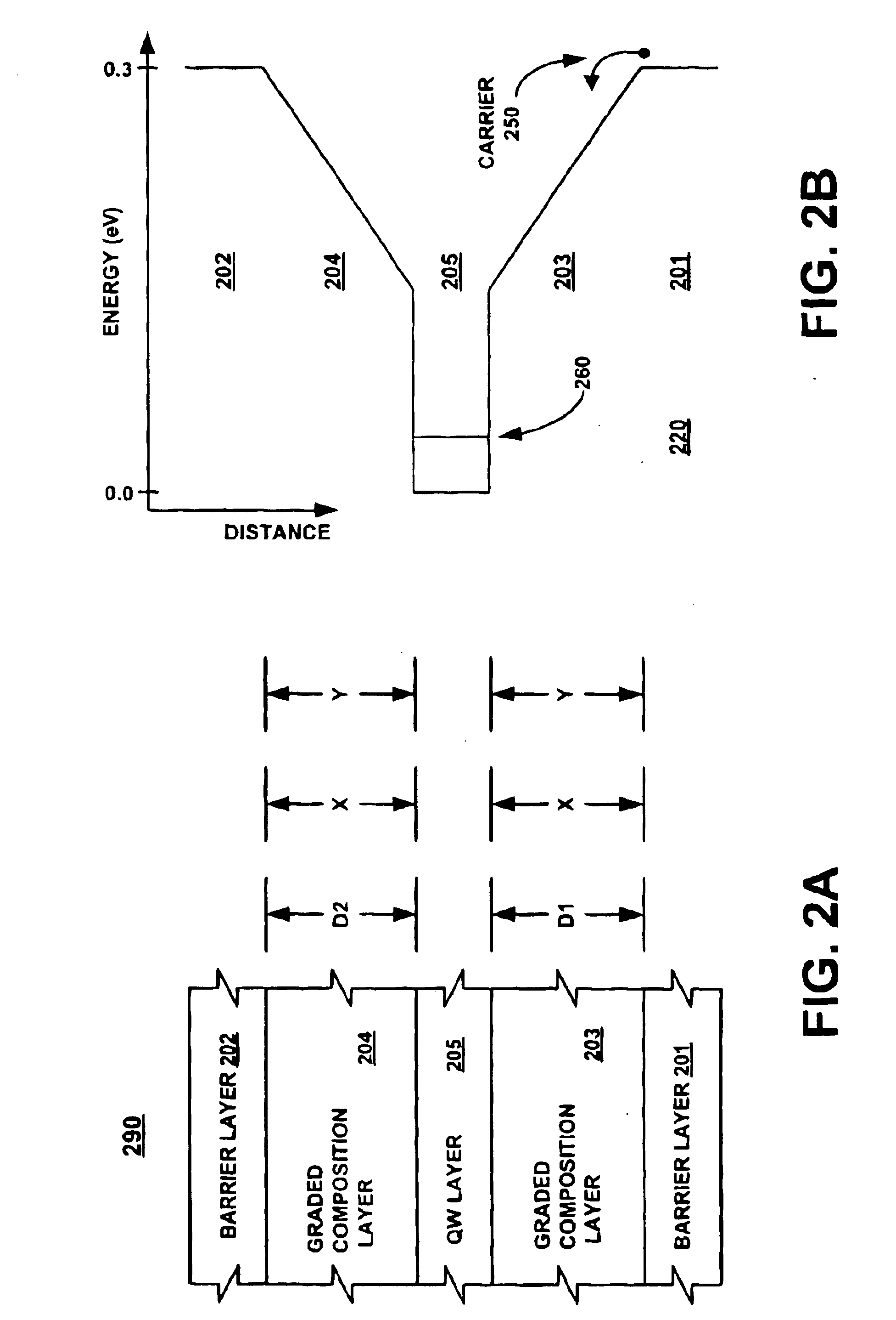
[0043]FIG. 2A is a cross-sectional view of a quantum well structure 290 of a light-emitting device according to the invention. FIG. 2B is a graph showing the conduction band profile 220 of the quantum well structure shown in FIG. 2A.

[0044]Turning first to FIG. 2A, quantum well structure 290 is composed of, in order, barrier layer 201, graded-composition layer 203, quantum well layer 205, graded-composition layer 204 and barrier layer 202. Quantum well layer 205 is a layer of a semiconductor material that has a relatively low bandgap energy. Barrier layers 201 and 202 are each a layer of a semiconductor material and have a higher bandgap energy than that of the quantum well layer 205.

[0045]Graded-composition layers 203 and 204 are each a layer of a semiconductor material whose composition is not uniform through the thickness of the layer. The graded-composition layers 203 and 204 have a thickness of D1 and D2, respectively. The thickness D1 and the thickness D2 can be substantially e...

second embodiment

[0056]The discussion now turns to FIG. 3A, which is a cross-sectional view of a quantum well structure 390 of a light-emitting device according to the invention. FIG. 3B is a graph showing the conduction band profile 320 of the quantum well structure shown in FIG. 3A.

[0057]Turning first to FIG. 3A, quantum well structure 390 is composed of, in order, barrier layer 301, intermediate composition layer 303, quantum well layer 305, intermediate composition layer 304 and barrier layer 302. Quantum well layer 305 is a layer of a semiconductor material that has a relatively low bandgap energy. Barrier layers 301 and 302 are each a layer of a semiconductor material and have a higher bandgap energy than that of the quantum well layer 305.

[0058]Intermediate composition layers 303 and 304 are each a layer of a semiconductor material whose composition remains relatively constant through the thickness of the layer. The material of the intermediate composition layers 303 and 304 has a bandgap ene...

third embodiment

[0067]Reference is now made to FIG. 4A, which is a cross-sectional view of a quantum well structure 400 of a light-emitting device according to the invention. FIG. 4B is a graph showing the conduction band profile 420 of the quantum well structure shown in FIG. 4A.

[0068]Referring first to FIG. 4A, quantum well structure 400 defines two quantum wells defined by quantum well structures 490 and 491. However, the present invention can be utilized with more or fewer than two quantum wells. Quantum well structure 490 is composed of, in order, barrier layer 401, quantum well layer 406, graded-composition layer 404, and barrier layer 402. Quantum well structure 491 is composed of, in order, barrier layer 402, quantum well layer 407, graded-composition layer 405, and barrier layer 403. Because quantum wells 490 and 491 are contiguous, they share the barrier layer 402. The graded-composition layers 404 and 405 have thicknesses D5 and D6, respectively. The thicknesses D5 and D6 can be substant...


PUM


Abstract

Light-emitting devices are described. One example of a light-emitting device includes a first barrier layer and a second barrier layer, and a quantum well layer located between the first and second barrier layers. The first and second barrier layers are composed of gallium arsenide, and the quantum well layer is composed of indium gallium arsenide nitride. A first layer is located between the quantum well layer and the first barrier layer. The first layer has a bandgap energy between that of the first barrier layer and that of the quantum well layer. Another example of a light-emitting device includes a quantum well and a carrier capture element adjacent the quantum well. The carrier capture element increases the effective carrier capture cross-section of the quantum well.

Description

TECHNICAL FIELD[0002]Embodiments of the present invention generally relate to light-emitting devices.BACKGROUND ART[0003]Light-emitting devices such as vertical-cavity surface-emitting lasers (VCSELs) are known in the art. In general, a VCSEL will employ one or more quantum wells to capture and confine carriers (electrons or holes), which subsequently radiatively recombine to generate light.[0004]Contemporary VCSELs generate light having a wavelength in the range of approximately 850-980 nanometers (nm). The ability to generate light at longer wavelengths is advantageous, especially in optical communications, and development of VCSELs that generate light at wavelengths of 1200 nm or more is ongoing. One type of longer-wavelength VCSEL includes an active region that incorporates a quantum well structure composed of one or more quantum well layers of indium gallium arsenide nitride (InGaAsN) and a corresponding number of barrier layers of gallium arsenide (GaAs). The quantum well(s) d...

Claims


Application Information

Patent Timeline
IPC IPC(8): H01L33/00H01S5/343H01L33/06H01L33/10H01L33/32
CPCB82Y20/00H01L33/32H01L33/06H01L33/105
Inventor BOUR, DAVID P.LEARY, MICHAEL H.CHANG, YING-LANSONG, YOON-KYUTAN, MICHAEL R. T.TAKEUCHI, TETSUYACHAMBERLIN, DANIELLE
Owner EPISTAR CORP
Why Eureka
Try Eureka